Semiconductor device and manufacturing method thereof

a technology of semiconductor devices and semiconductors, applied in semiconductor devices, diodes, electrical devices, etc., can solve problems such as inability to draw a performance, and achieve the effect of high avalanche resistance characteristics

Active Publication Date: 2007-10-11
NISSAN MOTOR CO LTD
View PDF22 Cites 40 Cited by
  • Summary
  • Abstract
  • Description
  • Claims
  • Application Information

AI Technical Summary

Benefits of technology

[0007]However, in the conventional structure, when the heterojunction is formed simply by using polycrystalline silicon, the forward and reverse characteristics result in developing a tendency similar to the Schottky junction diode. Therefore, it is not possible to draw a performance, as an electric characteristic, different from that of the Schottky junction.
[0008]The present invention has been achieved in view of the above problems, and an object thereof is to provide a semiconductor device having a higher avalanche resistance characteristic as compared to a Schottky junction diode, and a manufacturing method thereof.
[0009]To achieve the abov

Problems solved by technology

Therefore, it is not possible to draw a performance, as an elect

Method used


Image

  • Semiconductor device and manufacturing method thereof
  • Semiconductor device and manufacturing method thereof
  • Semiconductor device and manufacturing method thereof

Examples


first embodiment

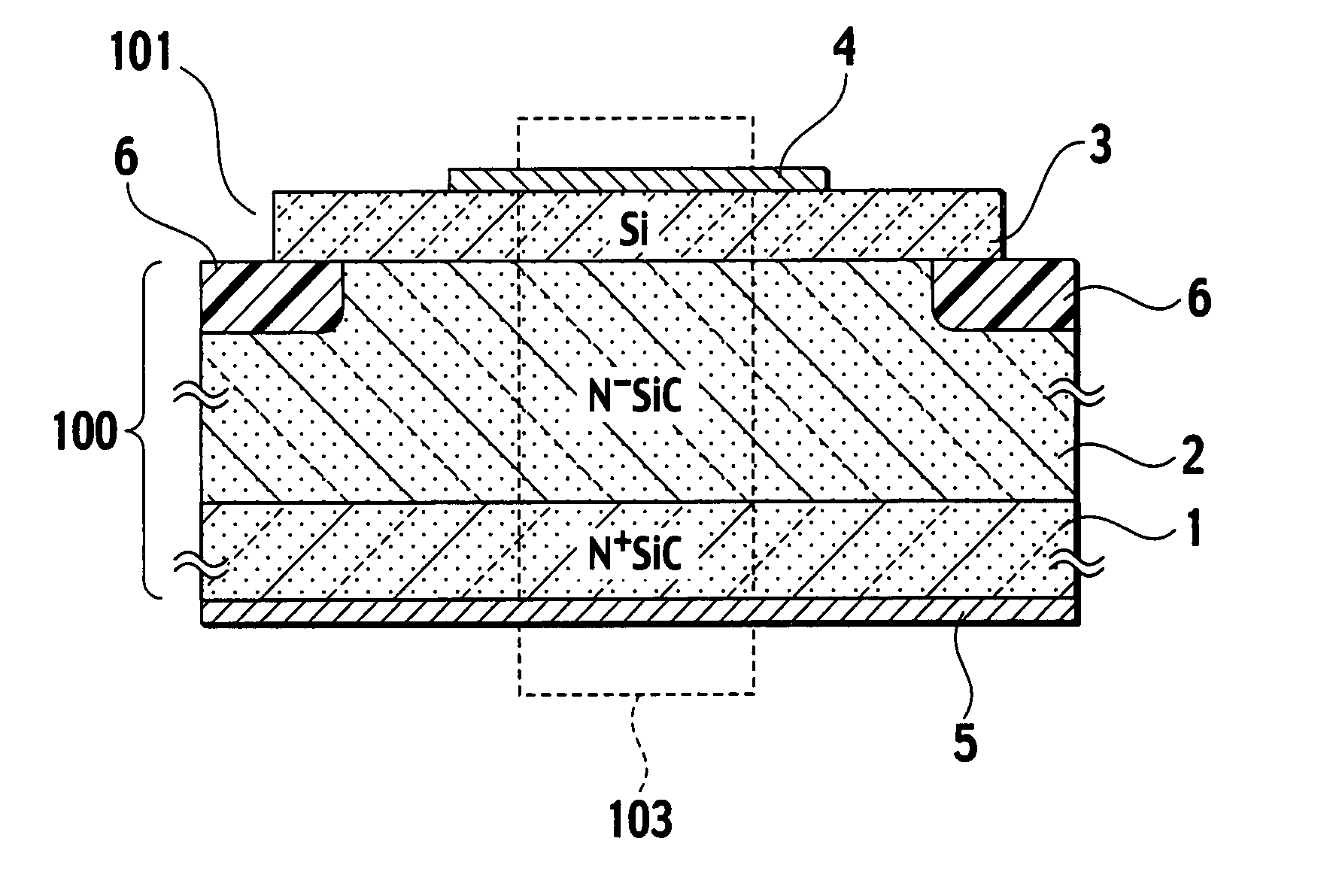
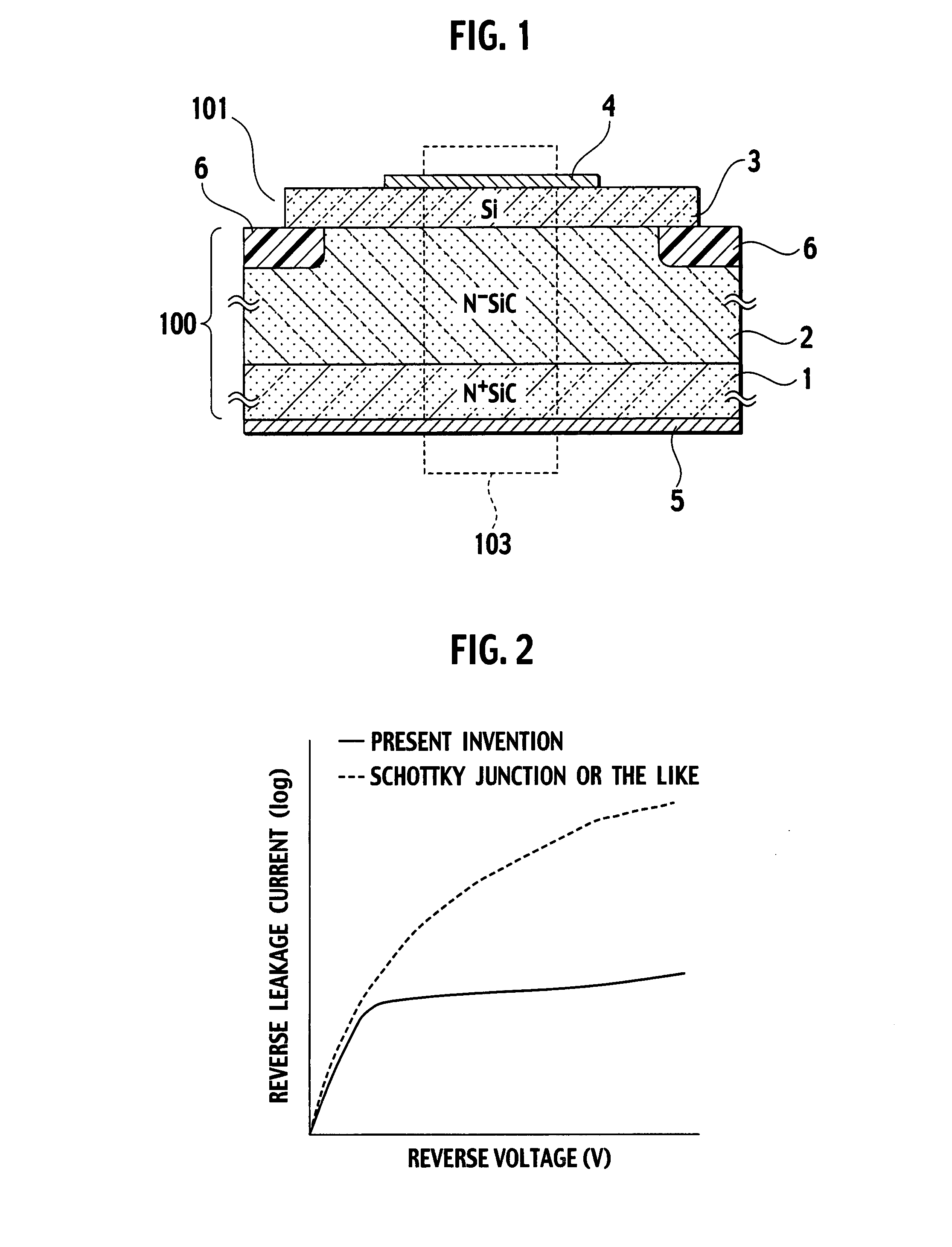
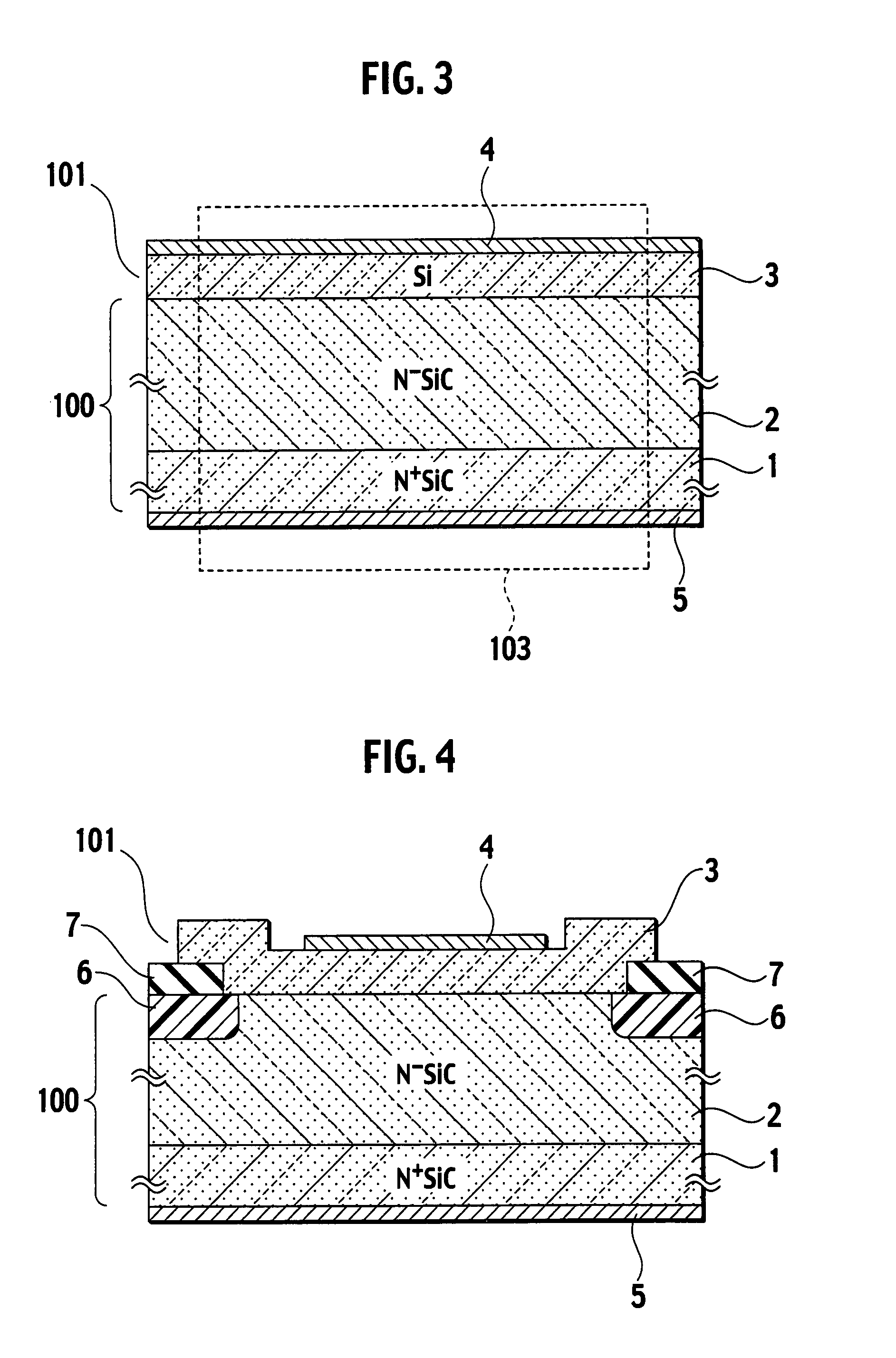
[0034]FIG. 1 is a cross-sectional view showing a configuration of a semiconductor device according to a first embodiment of the present invention. The semiconductor device of the first embodiment shown in FIG. 1 configures a heterojunction diode in which a heterojunction between silicon carbide and silicon is employed. Hereinafter, an explanation is given of a case where silicon carbide is employed as a substrate material of a first semiconductor region 100.

[0035]In FIG. 1, the first semiconductor region 100 is configured by a substrate material in which an N−-type drift region 2 is formed on an N+-type substrate region 1 of which the polytype of silicon carbide is 4H, for example. The substrate region 1, of which the resistivity is several to tens of mΩcm, and thickness is about tens or hundreds of micrometers, can be used. The drift region 2, of which N-type impurity density is 1015 to 1018 cm−3, and thickness is several to tens of micrometers, for example, can be used. In the fir...

second embodiment

[0099]FIG. 13 is a cross-sectional view showing the configuration of a semiconductor device according to a second embodiment of the present invention. A characteristic of the second embodiment shown in FIG. 13 is that the heterojunction diode having a high avalanche resistance, explained in the first embodiment including the first to eleventh modifications, is applied to a portion of a transistor.

[0100]In FIG. 13, the semiconductor device of the second embodiment is configured such that an N−-type drift region 22 is formed on an N+-type substrate region 21 of which the polytype of silicon carbide is 4H, for example; and first hetero semiconductor regions 23 comprised of P-type polycrystalline silicon and second hetero semiconductor regions 24 comprised of N-type polycrystalline silicon are formed so as to contact a main surface that opposes the junction surface, of the drift region 22, with the substrate 21.

[0101]A junction between the drift region 22, and the first and second heter...


PUM


Abstract

Impurity concentration of a second semiconductor region is set such that when a predetermined reverse bias is applied to a heterojunction diode configured by a first semiconductor region and the second semiconductor region, a breakdown voltage at least in a heterojunction region other than outer peripheral ends of the heterojunction diode is a breakdown voltage of a semiconductor device.

Description

BACKGROUND OF THE INVENTION[0001]1. Field of the Invention[0002]The present invention relates to a semiconductor device including a high resistance heterojunction diode and a manufacturing method thereof.[0003]2. Description of the Related Art[0004]Conventionally, a technique disclosed in Japanese Patent Application Laid-open No. 2003-318413 has been known as a similar technique of the present invention. In Japanese Patent Application Laid-open No. 2003-318413, an N-type polycrystalline silicon region is formed in a contacting manner on one main surface of a semiconductor base substrate formed with an N−-type epitaxial region on an N+-type substrate region, and the epitaxial region and the N-type polycrystalline silicon region form a heterojunction. On the rear surface of the N+-type substrate region, a rear surface electrode is formed.[0005]In the conventional technique thus configured, when the rear surface electrode is a cathode and the polycrystalline silicon region is an anode,...

Claims


Application Information

Patent Timeline
IPC IPC(8): H01L33/00H01L29/861H01L29/80H01L21/28H01L21/329H01L29/417H01L29/47H01L29/868H01L29/872
CPCH01L29/0619H01L29/1608H01L29/6606H01L29/7802H01L29/7808H01L29/165H01L29/8083H01L29/861H01L29/8618H01L29/872H01L29/7828H01L29/7811H01L31/109
Inventor HAYASHI, TETSUYAHOSHI, MASAKATSUSHIMOIDA, YOSHIOTANAKA, HIDEAKIYAMAGAMI, SHIGEHARU
Owner NISSAN MOTOR CO LTD
Why Eureka
Try Eureka