High temperature anodic bonding apparatus

an anodic bonding and high temperature technology, applied in the field of anodic bonding apparatus, can solve the problems that the process does not generally work with glass or glass-ceramic substrates, and the conventional techniques for anodic bonding of a semiconductor layer to a glass or glass-ceramic substrate do not adequately address the above process variables

Inactive Publication Date: 2007-10-25
CORNING INC
View PDF2 Cites 27 Cited by
  • Summary
  • Abstract
  • Description
  • Claims
  • Application Information

AI Technical Summary

Benefits of technology

[0018] In accordance with one or more further embodiments of the present invention, a bonding plate mechanism (for use in anodic bonding of first and second material sheets together) includes: a heating disk including first and second spaced apart surfaces and operable to produce heat in response to electrical power; a thermal spreader directly or indirectly coupled to the second surface of the heating disk and operable to at least channel heat from the heating disk, and impart voltage, to the first material sheet; and at least one cooling channel in thermal communication with the

Problems solved by technology

Notably, this process does not generally work with glass or glass-ceramic substrates because much higher temperatures are required for bonding some glass and glass-ceramic s

Method used


Image

  • High temperature anodic bonding apparatus
  • High temperature anodic bonding apparatus
  • High temperature anodic bonding apparatus

Examples


Embodiment Construction

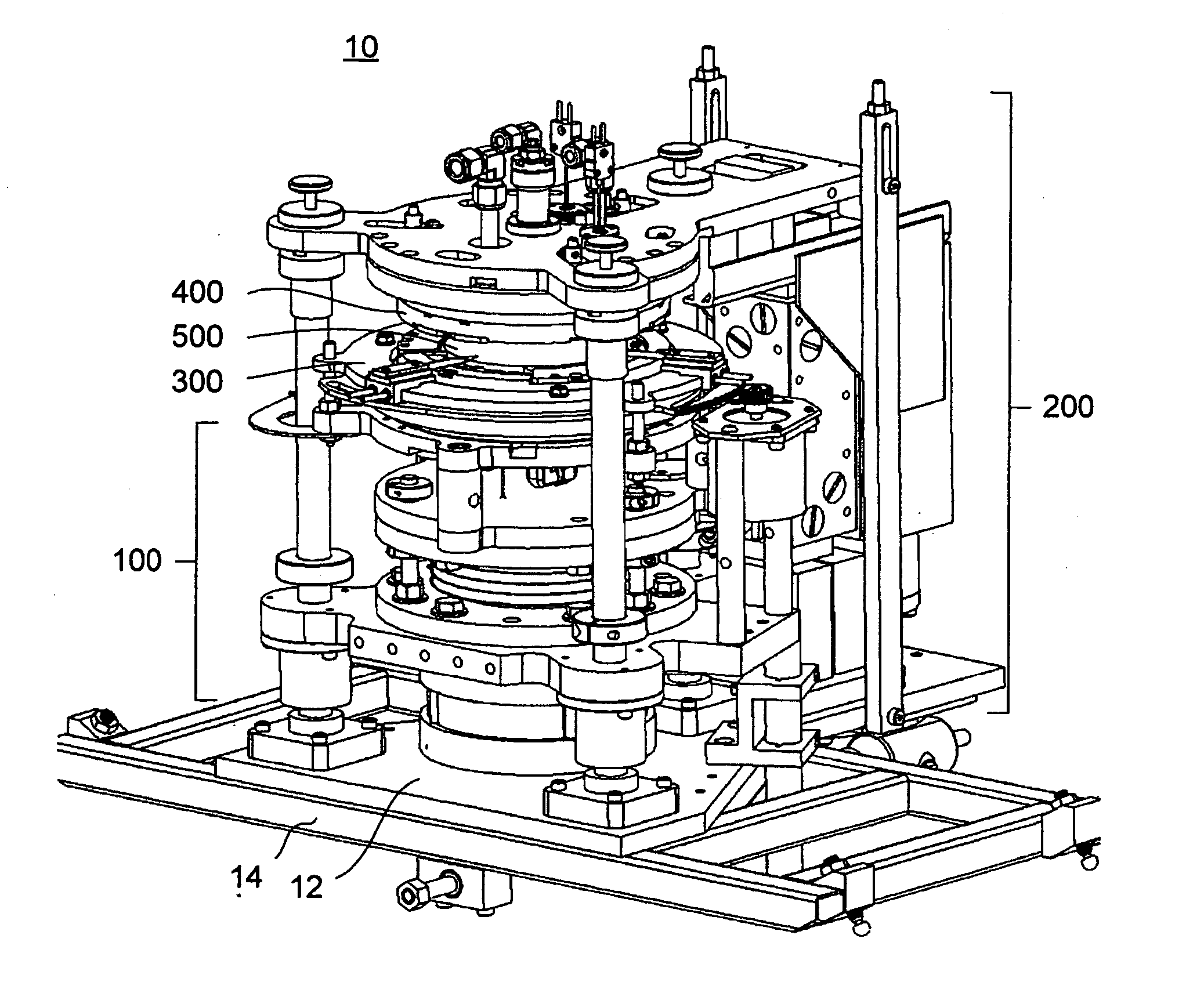
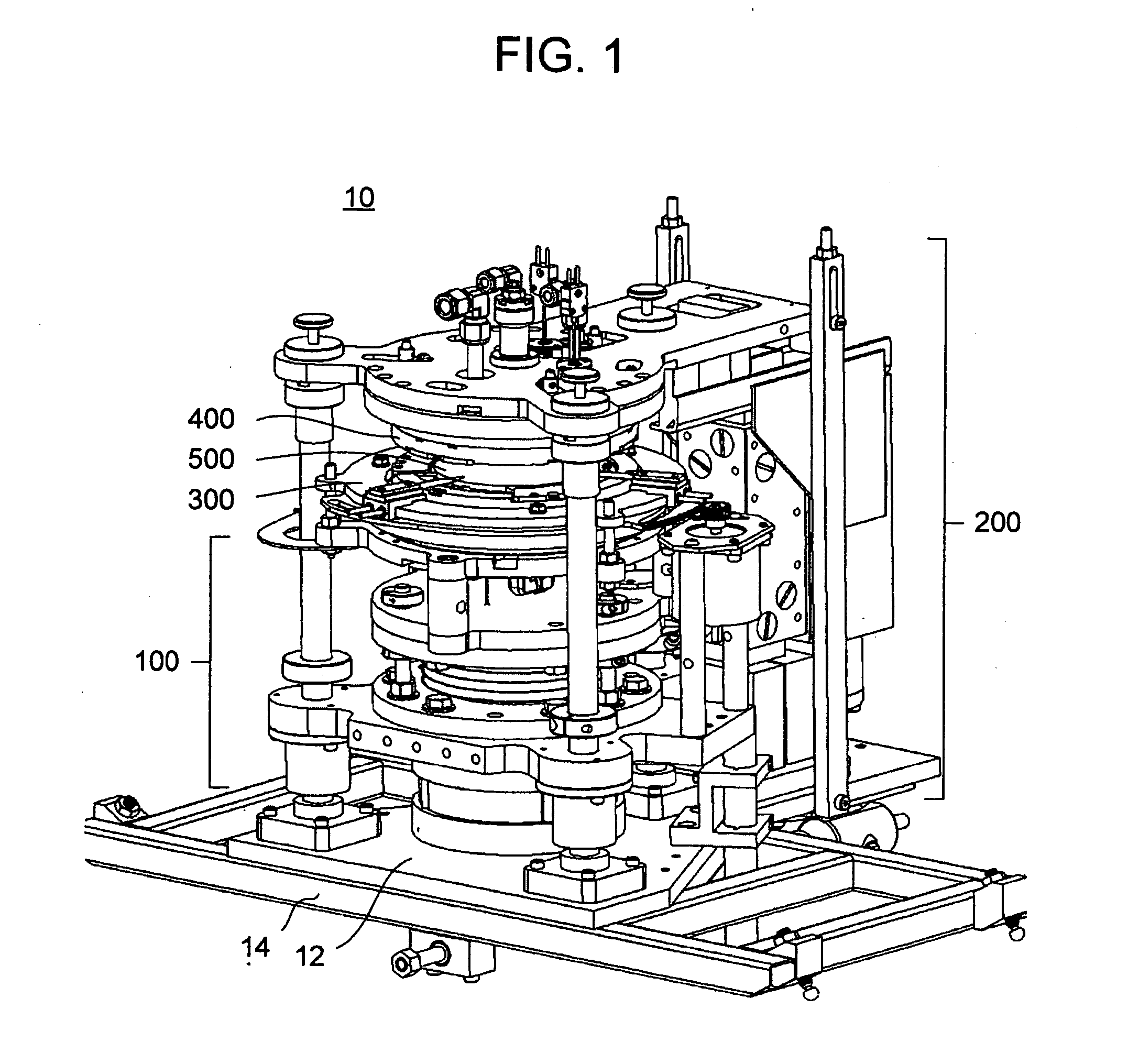
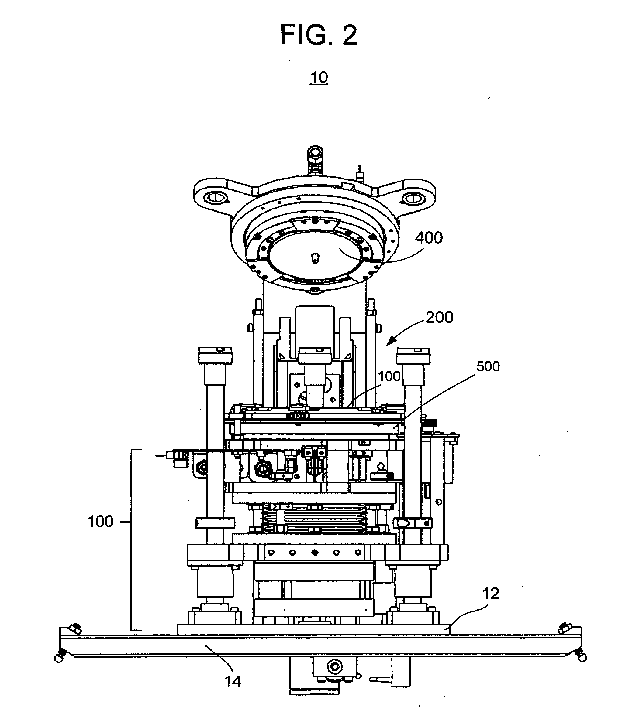
[0054] With reference to the drawings, wherein like numerals indicate like elements, there is shown in FIG. 1 a perspective view of a bonding apparatus 10 in accordance with one or more embodiments of the present invention. In this embodiment, the bonding apparatus is an integrated processing system capable of anodically bonding two material sheets of an SOI structure at temperatures above conventional bonding temperatures, e.g., above 600° C. and approaching and / or exceeding 1000° C. (It is noted that the bonding apparatus 10 is also capable of anodic bonding at conventional temperatures.) For purposes of illustration (but not limitation), an SOI structure will be described herein as a suitable work piece upon which the bonding apparatus 10 operates (e.g., in producing the SOI structure). Also for purposes of discussion (but not limitation), the particular SOI structure discussed hereinbelow as a work piece will be an SOG structure formed by bonding a semiconductor donor wafer (suc...


PUM


Abstract

An anodic bonding apparatus includes: a first bonding plate mechanism operable to engage a first material sheet, and to provide at least one of controlled heating, voltage, and cooling thereto; a second bonding plate mechanism operable to engage a second material sheet, and to provide at least one of controlled heating, voltage, and cooling thereto; a pressure mechanism operatively coupled to the first and second bonding plate mechanisms and operable to urge the first and second bonding plate mechanisms toward one another to achieve controlled pressure of the first and second material sheets against one another along respective surfaces thereof; a control unit operable to produce control signals to the first and second bonding plate mechanisms and the pressure mechanism to provide heating, voltage, and pressure profiles sufficient to achieve anodic bonding between the first and second material sheets.

Description

CROSS REFERENCE TO RELATED APPLICATION [0001] This application claims priority to U.S. Provisional Patent Application Ser. No. 60 / 793,976, filed Apr. 21, 2006 by Raymond C. Cady, entitled “A BONDING PLATE MECHANISM FOR USE IN ANODIC BONDING,” now pending, which is incorporated herein by reference in its entirety.BACKGROUND [0002] The present invention relates to an apparatus for manufacturing, for example, a semiconductor-on-insulator (SOI) structure using an anodic bonding technique. [0003] To date, the semiconductor material most commonly used in semiconductor-on-insulator structures has been silicon, and the abbreviation “SOI” has been applied to such structures. SOI technology is becoming increasingly important for high performance thin film transistors, solar cells, and displays, such as, active matrix displays. [0004] For ease of presentation, the following discussion will at times refer to SOI structures, however, such references to this particular type of structure are made ...

Claims


Application Information

Patent Timeline
IPC IPC(8): D06F75/26
CPCH01L21/67092H01L21/76254H01L21/67144H01L21/67121H01L21/02H01L27/12
Inventor CADY, RAYMOND C.LAKOTA, ALEXANDERLOCK, WILLIAM EDWARDTHOMAS, JOHN CHRISTOPHERCOSTELLO, JOHN JOSEPH III
Owner CORNING INC
Why Eureka
Try Eureka