Printed circuit board minimizing undesirable signal reflections in a via and methods therefor

a printed circuit board and signal reflection technology, applied in the direction of printed element electric connection formation, printed circuit non-printed electric component association, electrical apparatus construction details, etc., can solve the problems of increasing the manufacturing complexity of multi-layer pcb, affecting the signal quality of printed circuit boards, and adding undesirable cost and complexity. , to achieve the effect of increasing the density of the circuit board

Active Publication Date: 2007-11-08
AMPHENOL CORP
View PDF14 Cites 2 Cited by
  • Summary
  • Abstract
  • Description
  • Claims
  • Application Information

AI Technical Summary

Benefits of technology

[0012] It is an object of the invention to minimize undesirable signal reflections caused by resonant stub portions of conductive vias in a multi-layer PCB.
[0013] It is another object of the invention to provide an easily manufactured structure for making reliable electrical connection to a conductive trace on an inner layer of a multi-layer PCB.
[0015] It is still another object of the invention to provide a multi-layer PCB capable of improved aspect ratios.
[0017] Because the via does not have conductive plating, resonant stubs are not formed. A further advantage of the non-conductive via is that two conductive elements, such as contacts of two different electrical components, can be inserted into a single non-conductive via from opposite sides of the board in order to make direct electrical connection between the components and conductive traces on inner layers of the board. In this way, the circuit board density could be increased.

Problems solved by technology

One of the disadvantages associated with utilization of conductive vias relate to signal quality at high data rates.
The resulting buried vias are inaccessible and increase the manufacturing complexity of the multi-layer PCB.
However, this technique requires additional manufacturing steps that add undesirable cost and complexity.

Method used


Image

  • Printed circuit board minimizing undesirable signal reflections in a via and methods therefor
  • Printed circuit board minimizing undesirable signal reflections in a via and methods therefor
  • Printed circuit board minimizing undesirable signal reflections in a via and methods therefor

Examples


Embodiment Construction

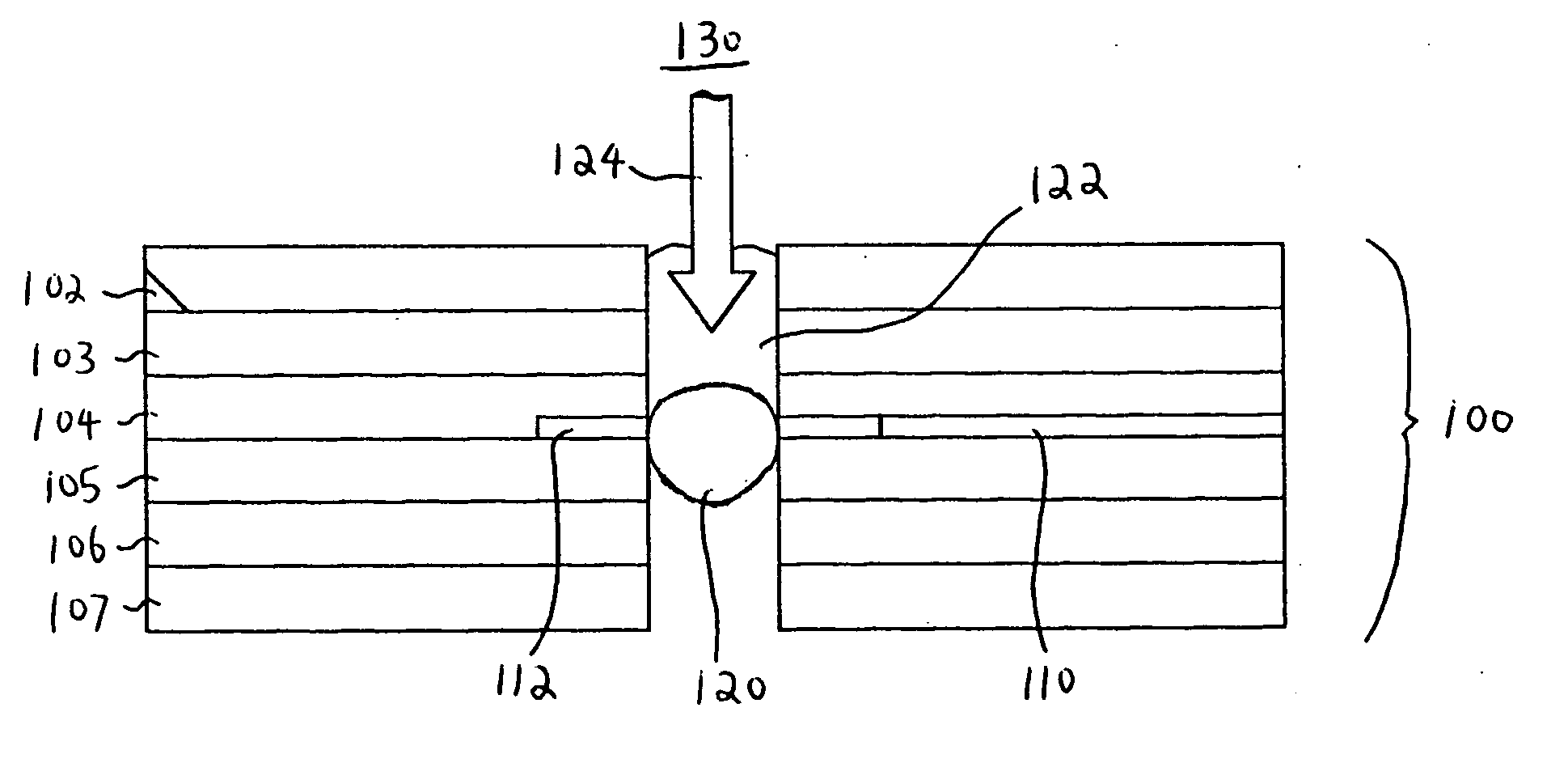
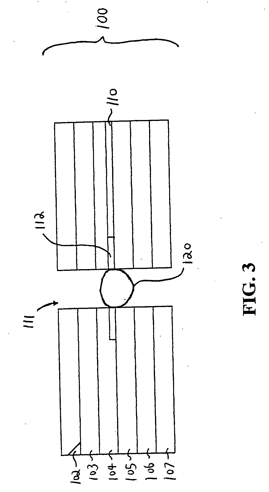
[0030]FIG. 3 is a partial cross-sectional view of a multi-layer printed circuit board 100 in accordance with the present invention. The multi-layer PCB 100 includes dielectric layers 102-107, with at least one of the dielectric layers having a conductive trace 110 formed on a surface in a conventional manner, such as by photolithography. The conductive trace 110 is adapted for carrying a high speed signal and has a conductive pad 112 connected thereto for facilitating electrical connection to the conductive trace 110.

[0031] A non-conductive via 111 in the form of a non-plated hole extends through at least a portion of the dielectric layers 102-107 to intersect at least one conductive trace on an inner layer of the PCB 100. In the illustrative embodiment of FIG. 3, the non-conductive via 111 extends through the entire PCB 100 and intersects the conductive pad 112 of the conductive trace 110, thereby exposing a portion of the pad 112 along the walls of the non-conductive via 111.

[00...


PUM

PropertyMeasurementUnit
thicknessaaaaaaaaaa
thicknessaaaaaaaaaa
diameteraaaaaaaaaa

Abstract

What is provided is a multi-layer PCB having a plurality of stacked dielectric layers, a conductor disposed on at least one of the plurality of dielectric layers, and a non-conductive via extending through at least a portion of the plurality of dielectric layers to intersect the conductor. A conductive body in an activated state is introduced into the non-conductive via, and upon contacting the conductor, the activated state conductive body adheres to the conductor. The activated state conductive body is then effected to a deactivated state, wherein the conductive body is affixed to the conductor to provide an electrical connection thereto.

Description

BACKGROUND OF THE INVENTION [0001] This invention relates generally to printed circuit boards and more specifically to high speed printed circuit boards that minimize undesirable signal reflections in a via. [0002] As is known in the art, conductive traces are formed on a printed circuit board (“PCB”) for carrying data signals and power between components mounted on the board. Space considerations often require the use of multi-layer PCBs including multiple layered dielectric substrates with conductive traces or planes formed on each substrate. The layered substrates are held together to make a PCB that has conductive traces on different levels within the board. [0003] In order to interconnect conductive traces on different layers, conductive vias extend between layers of the multi-layer PCB. For this purpose, conductive vias intersect vertically aligned pads joined to conductive traces on different layers. Conductive vias also interconnect components mounted on the board to conduct...

Claims


Application Information

Patent Timeline
Patent Type & Authority Applications(United States)
IPC IPC(8): H05K1/02H05K1/00H05K3/32H05K3/34H05K3/40
CPCH05K1/0298Y10T29/49139H05K3/3447H05K3/4038H05K3/4046H05K3/4069H05K2201/0305H05K2201/0919H05K2201/10234H05K2201/1059H05K2201/10992H05K2203/041H05K2203/1446Y10T29/49165Y10T29/4913Y10T29/49147H05K3/321
Inventor KHILCHENKO, LEON M.GAILUS, MARK W.
Owner AMPHENOL CORP
Why Eureka
Try Eureka