Method of thinning a wafer

Inactive Publication Date: 2007-11-08
TOUCH MICRO SYST TECH
View PDF5 Cites 15 Cited by
  • Summary
  • Abstract
  • Description
  • Claims
  • Application Information

AI Technical Summary

Benefits of technology

[0005]It is therefore an objective of the present invention to provide a method of thinning a

Problems solved by technology

Because the method of thinning a wafer is limited by the supporting mechanism, such as an electrostatic chuck, the wafers can only

Method used


Image

  • Method of thinning a wafer
  • Method of thinning a wafer
  • Method of thinning a wafer

Examples


Embodiment Construction

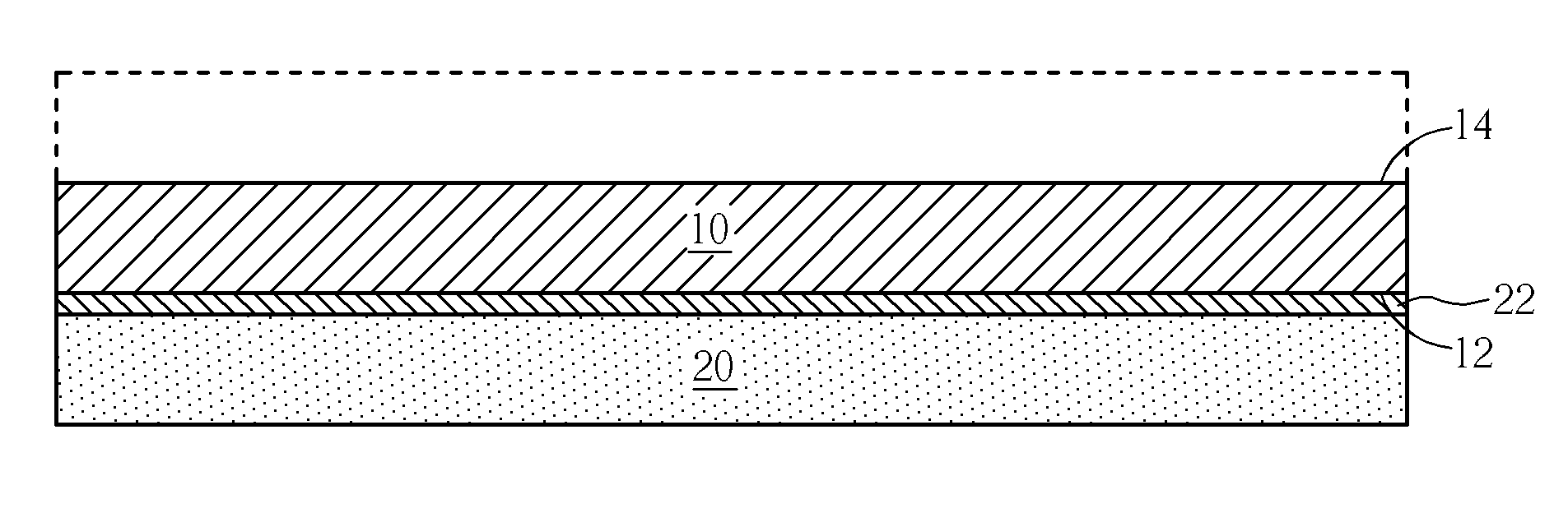
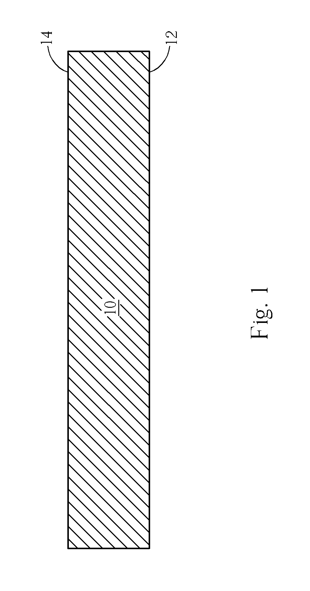
[0009]Please refer to FIGS. 1 to 10. FIGS. 1 to 10 are schematic diagrams illustrating a method of thinning a wafer according to a preferred embodiment of the present invention. As shown in FIG. 1, a wafer 10 is first provided, the wafer including a front surface 12 and a back surface 14. In this preferred embodiment, the wafer 10 is a wafer that already includes the needed semiconductor components or micro-electromechanical components (not shown in the figure) in its front surface 12, and also requires thinning. However, the method of the present invention is not limited by this preferred embodiment, and can be applied to any wafer thinning process in semiconductor processes or in micro-electromechanical processes.

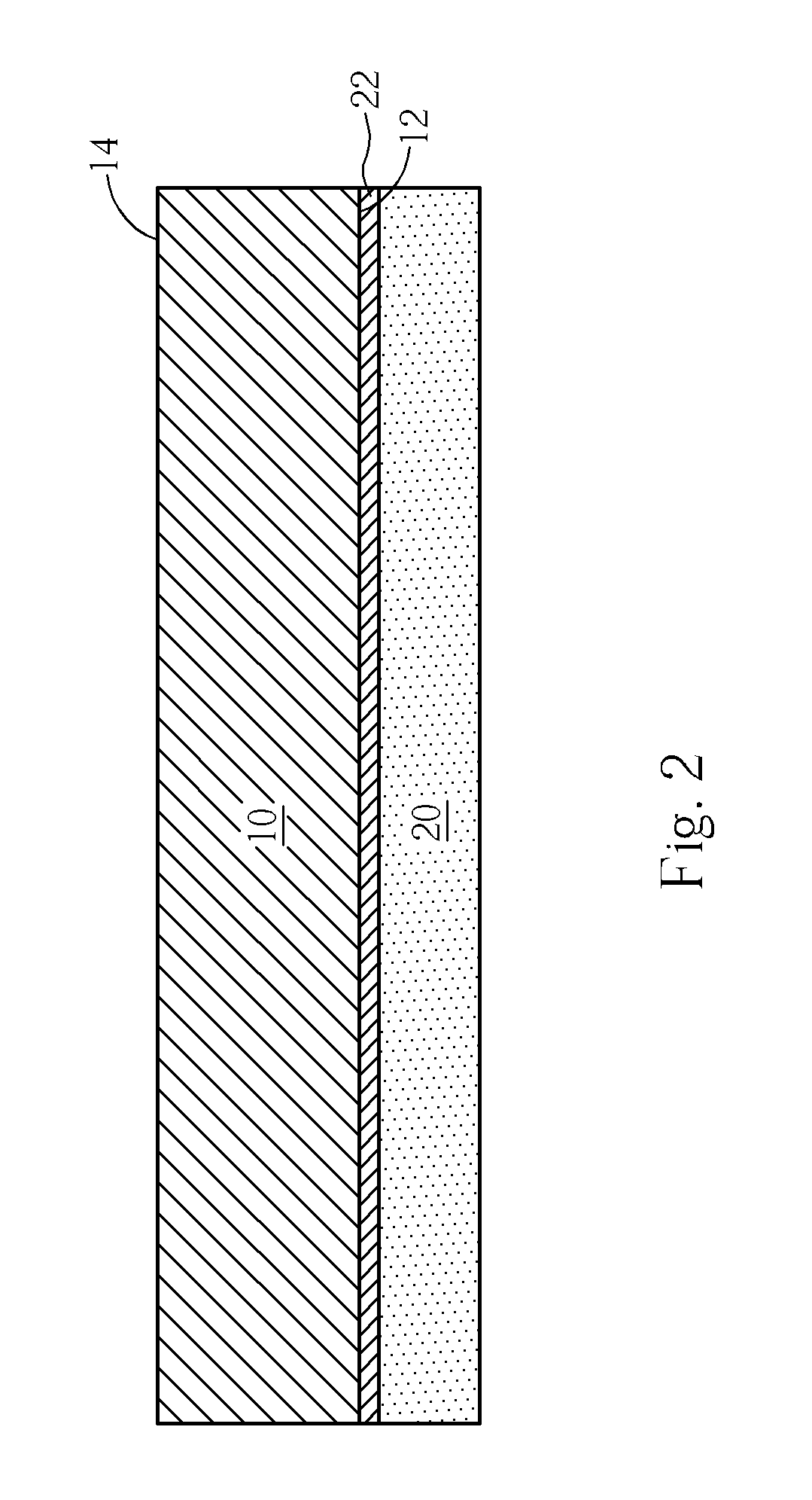
[0010]As shown in FIG. 2, a carrier wafer 20, such as a semiconductor wafer, a glass wafer, a plastic wafer, or a silicon wafer, is subsequently provided, and the front surface 12 of the wafer 10 is bonded to a surface of the carrier wafer 20 with a bonding layer 22. The ...


PUM


Abstract

A method of thinning a wafer. A wafer is provided, and the front surface of the wafer is bonded to a carrier wafer with a bonding layer. The bonding layer is a thermal release tape or a UV tape. Subsequently, a wafer thinning process is performed to thin the wafer from the back surface.

Description

BACKGROUND OF THE INVENTION[0001]1. Field of the Invention[0002]The invention relates to a method of thinning a wafer, and more particularly, to a method of fixing a wafer onto a carrier wafer with a bonding layer, such as a thermal release tape or an ultraviolet (UV) tape, so as to increase the minimum thickness of wafer thinning.[0003]2. Description of the Prior Art[0004]In consideration of designated functions or desired size, many semiconductor components and micro-electromechanical components have to perform a wafer thinning process, so that the wafers are thinned into the desired sizes. Because the method of thinning a wafer is limited by the supporting mechanism, such as an electrostatic chuck, the wafers can only be thinned to a thickness of about 100 micrometers as the extreme. When the wafer is excessively thinned, breaks can easily occur.SUMMARY OF THE INVENTION[0005]It is therefore an objective of the present invention to provide a method of thinning a wafer, so as to pr...

Claims


Application Information

Patent Timeline
IPC IPC(8): H01L21/30
CPCH01L21/78
Inventor KUO, CHIH-PING
Owner TOUCH MICRO SYST TECH
Why Eureka
Try Eureka