Fingerprinting Device

Inactive Publication Date: 2007-11-15
ASMAG HLDG
View PDF6 Cites 6 Cited by
  • Summary
  • Abstract
  • Description
  • Claims
  • Application Information

AI Technical Summary

Benefits of technology

[0003] The object of the invention is accordingly to construct a fingerprinting device of the type described at the

Problems solved by technology

The main drawback of this known fingerprinting device is the design costs caused by the use of light-sensitive elements based on inorganic semico

Method used


Image

  • Fingerprinting Device
  • Fingerprinting Device
  • Fingerprinting Device

Examples


Embodiment Construction

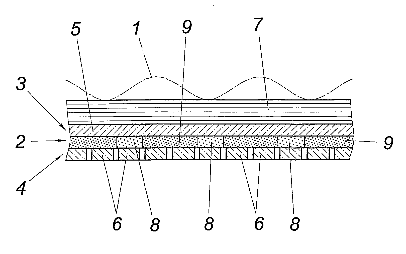
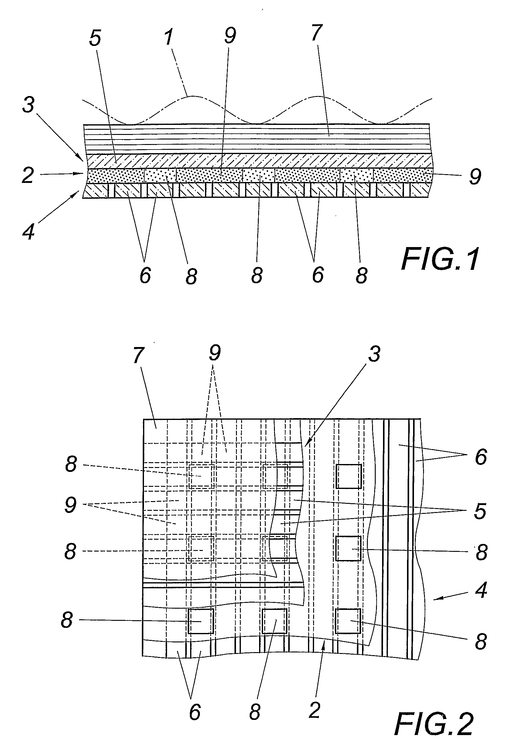
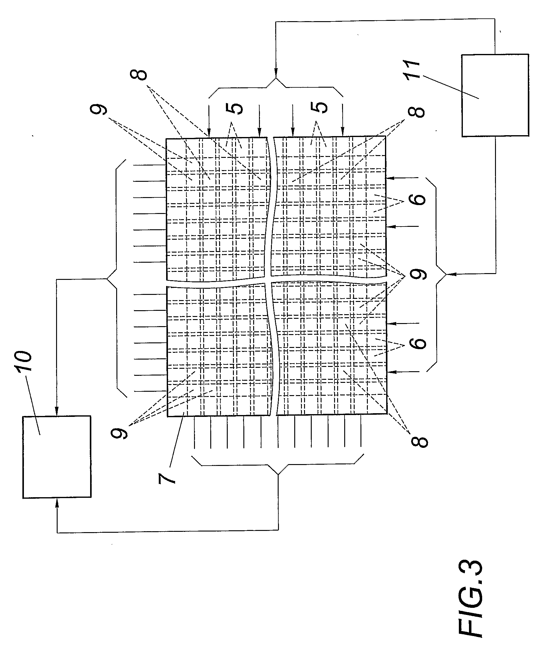
[0013] As may be seen, in particular, in FIG. 1 and 2, the illustrated device for recording a fingerprint 1 indicated in FIG. 1 by a broken line has a photoactive layer 2 adjoined by two electrode layers 3, 4 consisting of intersecting strip conductors 5, 6. The photoactive layer 2 is constructed on the basis of organic semiconductors, the charge movability of which parallel to the layer face is comparatively small, thus producing photoactive elements substantially separated from one another in the region of intersection of the strip conductors 5, 6. In order to be able, on the one hand, to illuminate the fingerprint 1 through a translucent top layer 7 forming a finger rest and, on the other hand, to detect the light reflected diffusely on the fingerprint 1 for imaging the fingerprint, individual regions of the photoactive layer 2 that are locally defined by the region of intersection of specific strip conductors 5, 6 are used as light-emitting elements 8 and the remaining regions a...


PUM


Abstract

Described is a fingerprinting device ( 1 ) with a translucent top layer ( 7 ) which forms a finger rest and on the side of which that is remote from the finger rest a layer, connected to an evaluation circuit ( 10 ), of light-sensitive elements ( 9 ) in a matrix arrangement and light-emitting elements ( 8 ) are provided. In order to provide advantageous design conditions, it is proposed that on the side of the top layer ( 7 ) that is remote from the finger rest there be arranged a photoactive layer ( 2 ) based on organic semiconductors between two electrode layers ( 3, 4 ) consisting of intersecting strip conductors ( 5, 6 ), of which the strip conductors ( 5 ) between the photoactive layer ( 2 ) and the top layer ( 7 ) are translucent, and that the photoactive layer ( 2 ) form the light-sensitive and the light-emitting elements ( 8, 9 ) in the region of intersection of the strip conductors ( 5, 6 ) of the two electrode layers ( 3, 4 ).

Description

FIELD OF THE INVENTION [0001] The invention relates to a fingerprinting device with a translucent top layer which forms a finger rest and on the side of which that is remote from the finger rest a layer, connected to an evaluation circuit, of light-sensitive elements in a matrix arrangement and light-emitting elements are provided. DESCRIPTION OF THE PRIOR ART [0002] In order to be able digitally to record a fingerprint, without firstly optically imaging the fingerprint using a lens system, it is known (WO 97 / 036544 A1) to arrange light-sensitive elements, preferably photodiodes or phototransistors, using thin-layer technology on a transparent carrier made of glass or quartz and to cover them with a light-emitting layer consisting, for example, of electroluminescent diodes. As the light-sensitive elements are arranged in rows in a matrix and the rows of elements are separated from one another by translucent gaps, light can be cast from the light-emitting layer, through the transluce...

Claims


Application Information

Patent Timeline
IPC IPC(8): G01J1/44G06K9/00H01L27/146H01L51/10
CPCG06K9/0004
Inventor PADINGER, FRANZSCHROTER, KLAUS G.
Owner ASMAG HLDG
Why Eureka
Try Eureka