Semiconductor device that is advantageous in complex stress engineering and method of manufacturing the same
- Summary
- Abstract
- Description
- Claims
- Application Information
AI Technical Summary
Benefits of technology
Problems solved by technology
Method used
Image

Examples
first embodiment
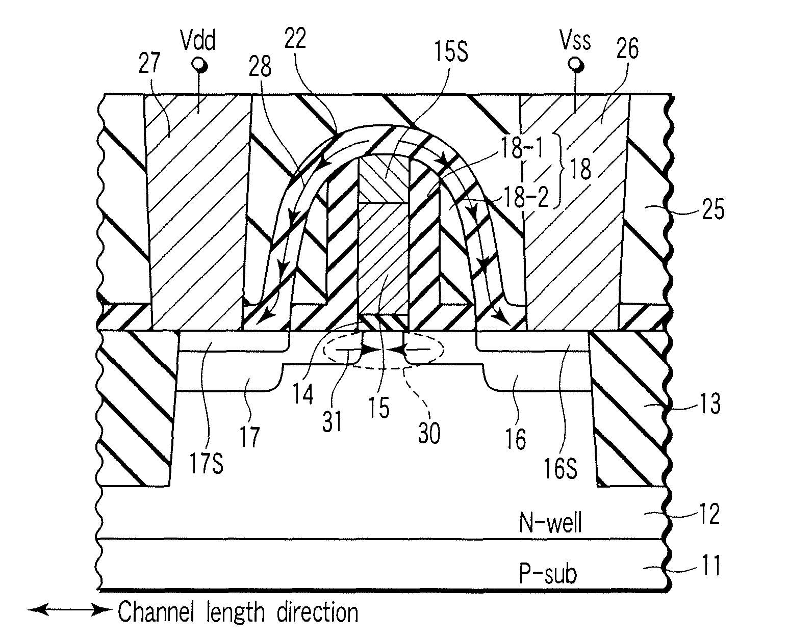
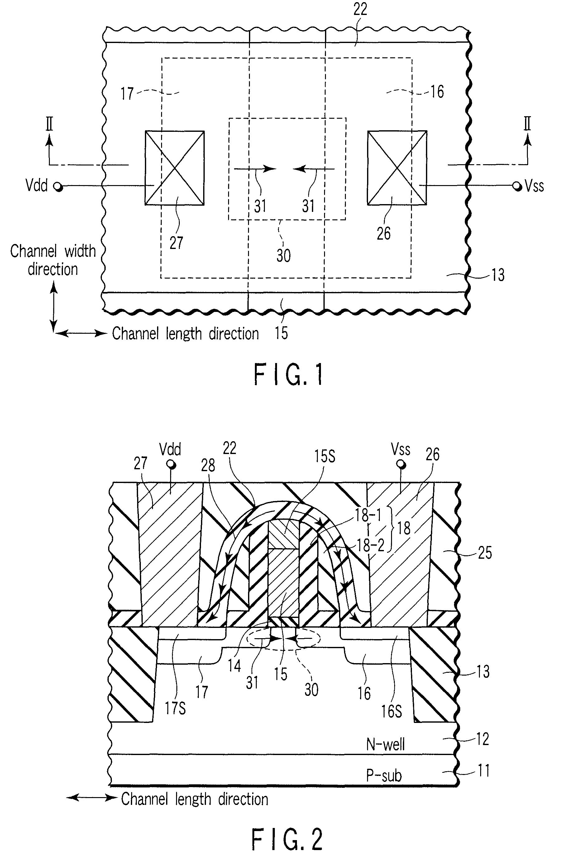
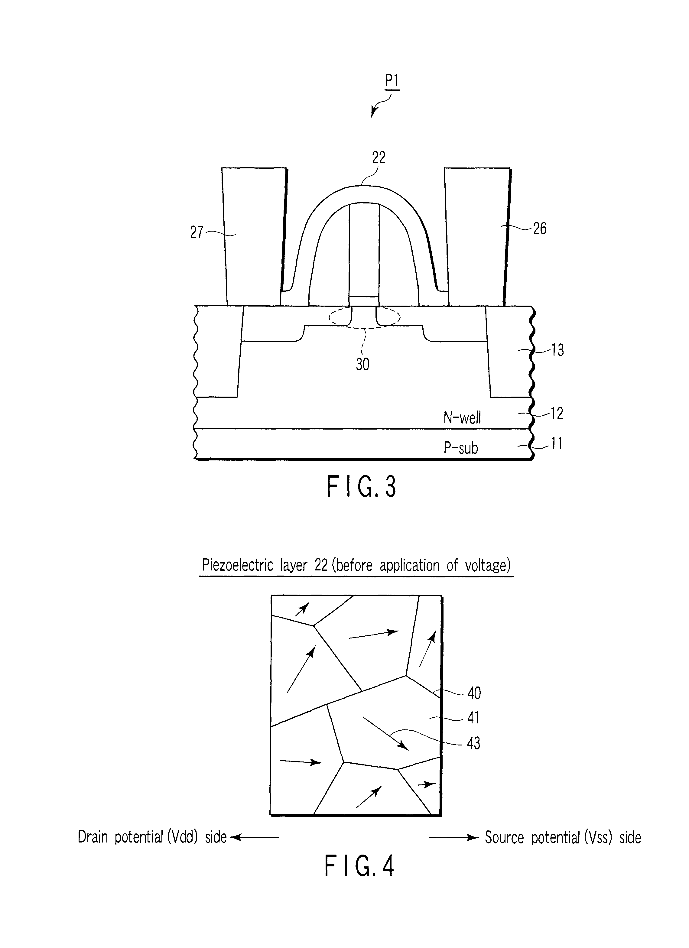
[0034]A semiconductor device according to a first embodiment of the present invention is described with reference to FIG. 1 and FIG. 2. FIG. 1 is a plan view that schematically shows a semiconductor device according to the first embodiment of the invention. FIG. 2 is a cross-sectional view taken along line II-II in FIG. 1.
[0035]As shown in FIGS. 1 and 2, a P-type MOS (metal oxide semiconductor) transistor (PMOS transistor) P1 is provided on an N-well 12 which is formed in a P-type semiconductor (e.g. silicon) substrate (P-sub) 11 that is isolated by a device isolation film 13.
[0036]The PMOS transistor P1 includes a gate insulation film 14, a gate electrode 15, a source 16, a drain 17, silicide layers 15S, 16S and 17S, and spacer insulation films 18-1 and 18-2.
[0037]The gate insulation film 14 is provided on the N-well 12. The gate electrode 15 is provided on the gate insulation film 14. The silicide layer 15S is provided on the gate electrode 15. The source 16 and drain 17 are provi...
second embodiment (
Example of Sol-gel Method)
[0070]Next, a semiconductor device according to a second embodiment of the invention is described with reference to FIG. 10 and FIG. 11. This embodiment relates to an example in which the piezoelectric layer 22, which has been described in the first embodiment, is fabricated by using a sol-gel method. A detailed description of the structure of the second embodiment is omitted since the structure is the same as that of the first embodiment.
[0071]To begin with, as shown in FIG. 10, using the same fabrication step as in the first embodiment, the gate structure, spacer 18, source 16, drain 17 and silicide layers 15S, 16S and 17S are formed on the N-well 12.
[0072]Referring to FIG. 11, a step of forming the piezoelectric layer (BaTiO3 layer) 22 on the above-described structure is described. Barium acetate and titanium tetra n-butoxide are dissolved in methanol solution so that a mixing ratio of Ba / Ti may become 1:1. Using acetic acid as catalyst in this case, an ...
third embodiment (
Example in which Stress is Applied to a Central Part of the Channel Region)
[0076]Next, a semiconductor device according to a third embodiment of the invention is described with reference to FIG. 12 and FIG. 13. FIG. 12 is a plan view showing the semiconductor device according to the third embodiment. FIG. 13 is a cross-sectional view taken along line IX-IX in FIG. 12. This embodiment relates to an example in which the piezoelectric layer 22, which has been described in the first embodiment, is formed on a central part of the channel region 30. A description of the parts common to those of the first embodiment is omitted here.
[0077]As shown in the Figures, a PMOS transistor P2 is provided on the N-well 12. The transistor P2 includes a piezoelectric layer (BaTiO3 layer) 22 which is electrically connected to the contact wiring lines 26 and 27 and is so formed as to cover the gate electrode 15 and the spacer. This piezoelectric layer 22 differs from that of the first embodiment in that ...
PUM
 Abstract
Description
Claims
Application Information