

Receptacles for inkjet deposited PLED/OLED devices and method of making the same
a technology of inkjet deposited pled/oled devices and pled/oled devices, which is applied in the direction of discharge tube luminescnet screens, discharge tube/lamp details, electric discharge lamps, etc., can solve the problems of complex and costly, high production process costs, and inflexible, and achieve less complex and cost-effective effects
- Summary
- Abstract
- Description
- Claims
- Application Information
AI Technical Summary
Benefits of technology
Problems solved by technology
Method used
Image

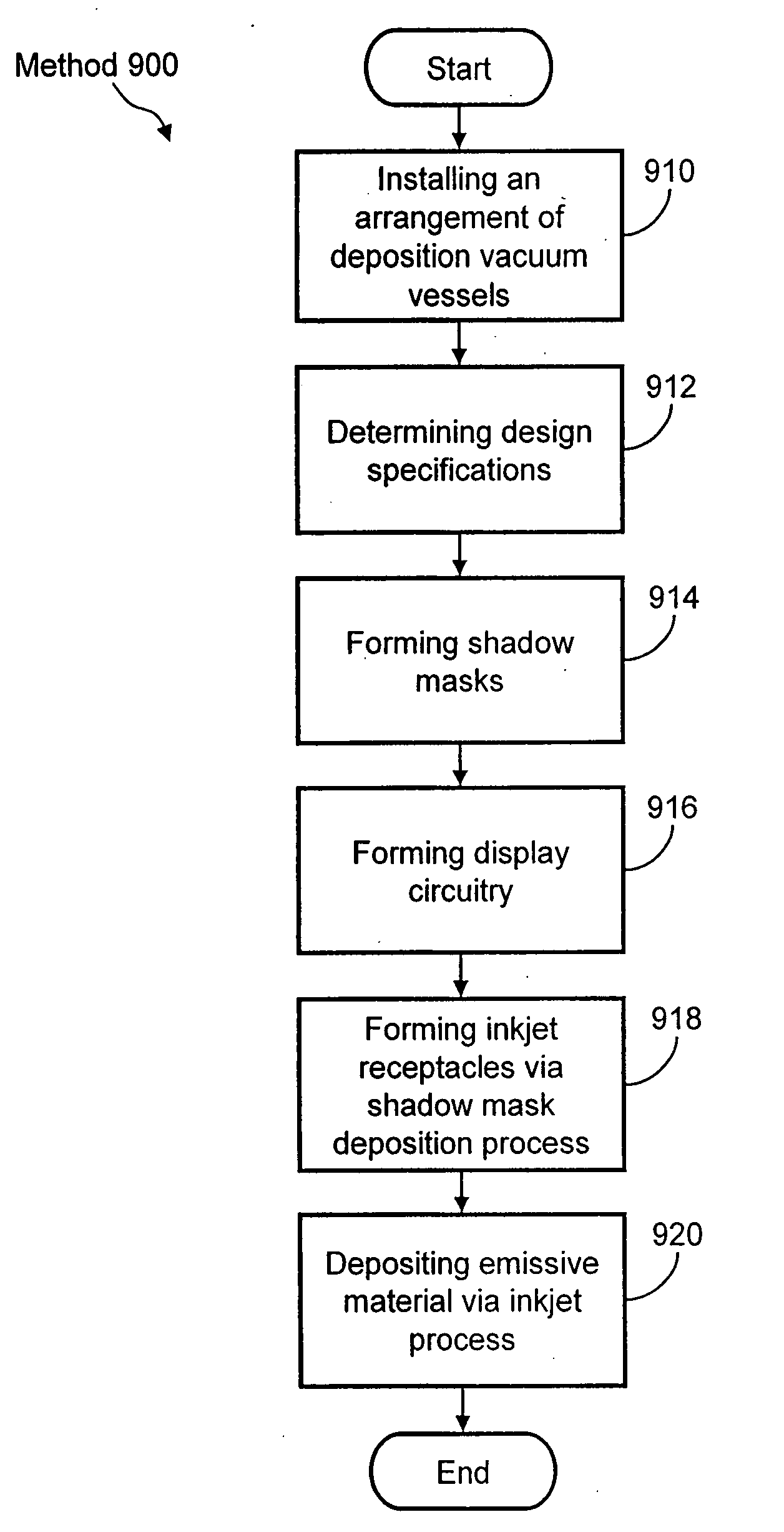
Examples
first embodiment
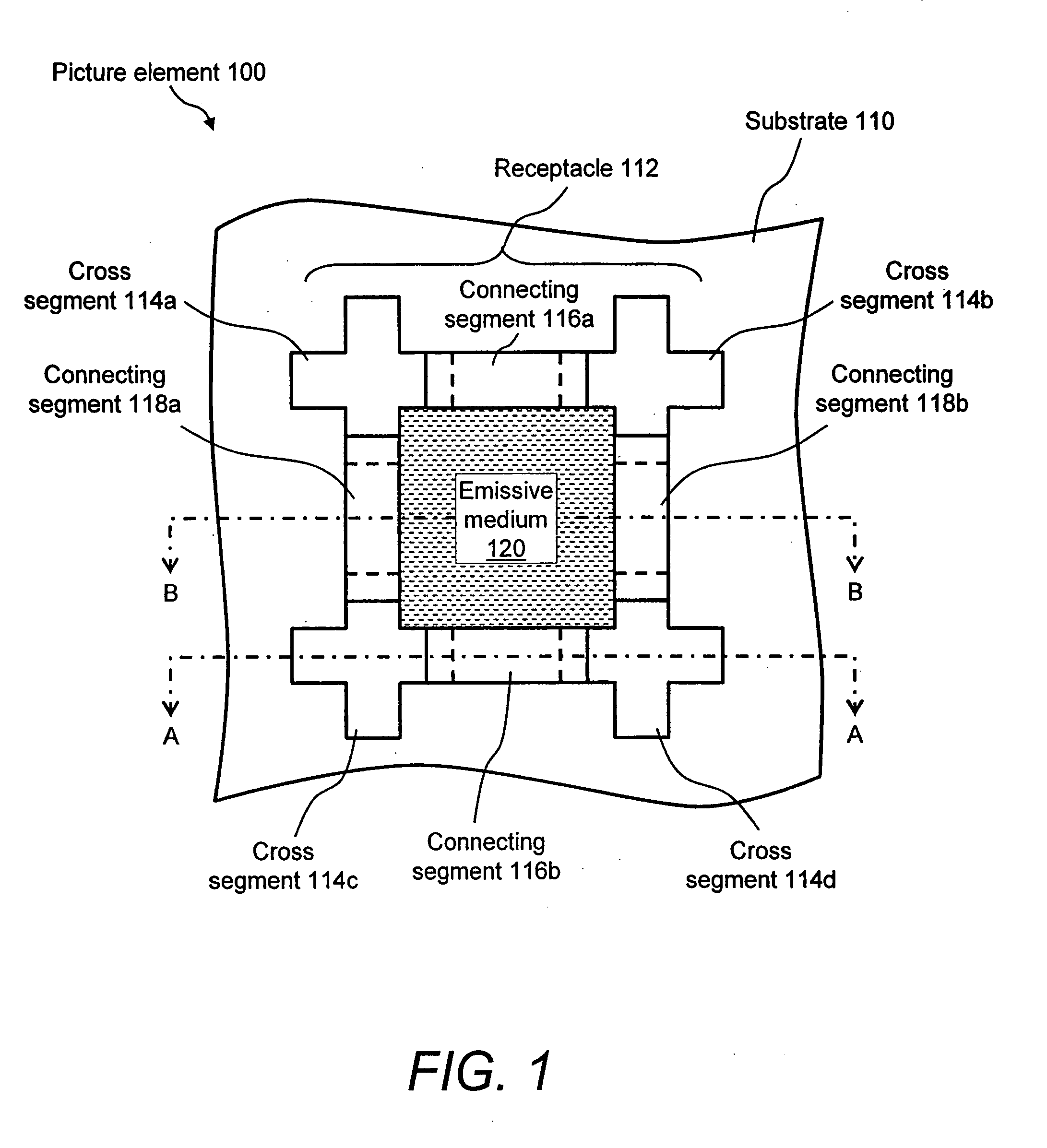
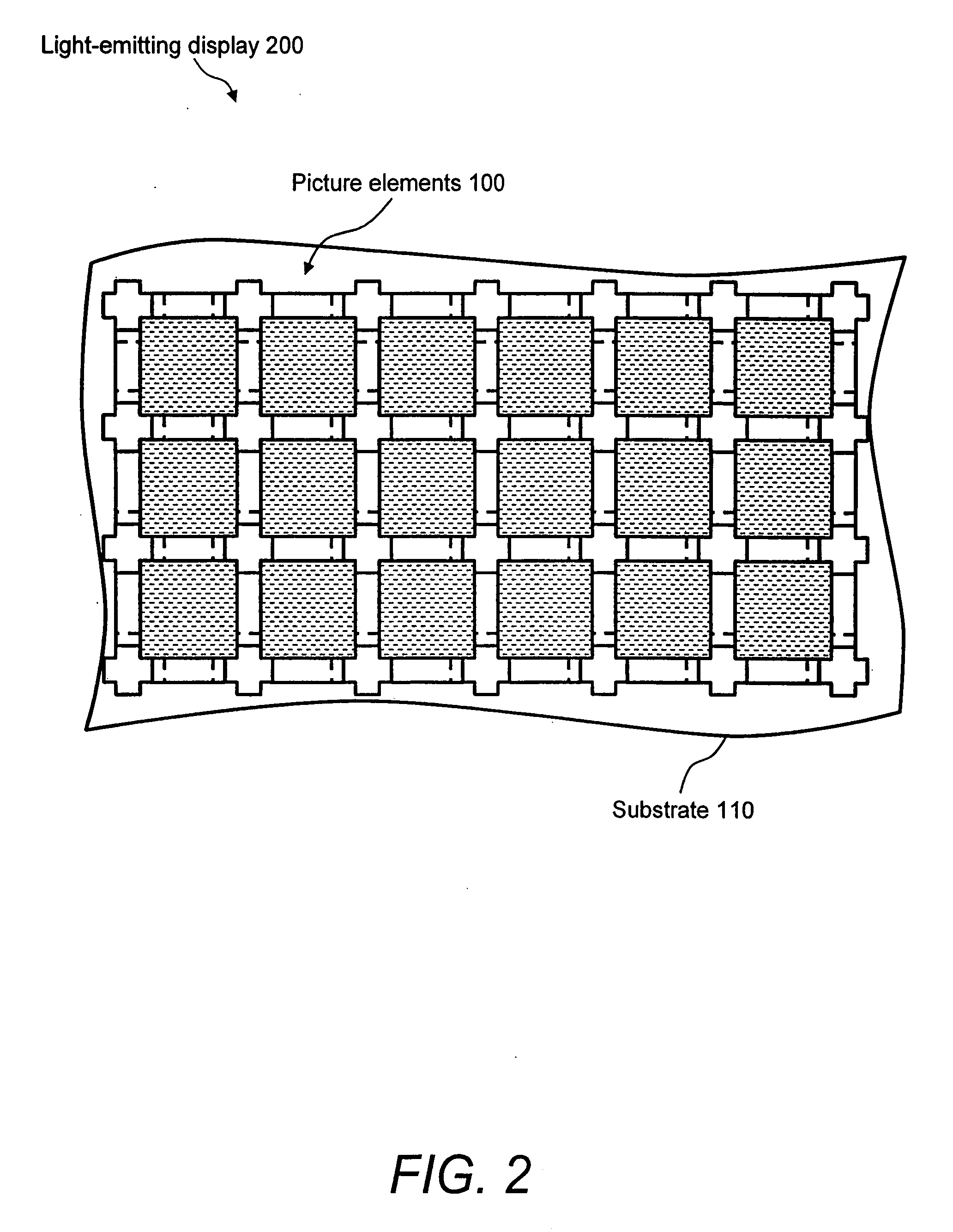
[0023]FIG. 1 illustrates a top view of a picture element 100 in accordance with the invention. Picture element 100 is a representative pixel of a flat-panel display, such as a PLED or OLED display. Picture element 100 includes a substrate 110 upon which is formed a receptacle 112. Receptacle 112 is formed by an arrangement of evaporated segments. Receptacle 112 is formed of a plurality of cross segments 114 arranged on a grid that are interconnected via a plurality of connecting segments 116 and connecting segments 118, which form the walls of receptacle 112 for retaining liquid solvent during an inkjet deposition process.
[0024] In this example, receptacle 112 is formed of a cross segment 114a, a cross segment 114b, a cross segment 114c, and a cross segment 114d, arranged on a grid as shown in FIG. 1. Cross segments 114a and 114b are interconnected via a connecting segment 116a to form a first wall of receptacle 112; cross segments 114c and 114d are interconnected via a connecting s...
second embodiment
[0046]FIG. 6 illustrates a top view of a picture element 600 in accordance with the invention. Picture element 600 is a representative pixel of a flat-panel display, such as a PLED or OLED display. Picture element 600 includes substrate 110, upon which is formed a receptacle 612. Receptacle 612 is formed by an arrangement of evaporated segments and is formed of a plurality of cross segments 614, arranged on a grid, that are interconnected via a plurality of connecting segments 616 and connecting segments 618, which form the walls of receptacle 612 for retaining liquid solvent during an inkjet deposition process.
[0047] In this example, receptacle 612 is formed of a cross segment 614a, a cross segment 614b, a cross segment 614c, and a cross segment 614d, arranged on a grid, as shown in FIG. 6. Cross segments 614a and 614b are interconnected via a connecting segment 616a to form a first wall of receptacle 612; cross segments 614c and 614d are interconnected via a connecting segment 616...
PUM
 Abstract
Description
Claims
Application Information