Optoelectronic device chip having a composite spacer structure and method making same

Active Publication Date: 2007-11-22
TAIWAN SEMICON MFG CO LTD +2
View PDF9 Cites 12 Cited by
  • Summary
  • Abstract
  • Description
  • Claims
  • Application Information

AI Technical Summary

Benefits of technology

[0012] A first object of the present invention is to provide an optoelectronic device chip in

Problems solved by technology

Such thick photoresist layer (unlike the photoresist layer used for patterning a semiconductor integrated circuit layer, which is typically in the range of about 1 μm) would result in severe wafer uniformity issue, typically ±(10-20)% thickness variation across the wafer due to spin coating and photoresist viscosity.
Such a huge difference is unacceptable because it would cause severe defocus issue when the pixel size is smaller t

Method used


Image

  • Optoelectronic device chip having a composite spacer structure and method making same
  • Optoelectronic device chip having a composite spacer structure and method making same
  • Optoelectronic device chip having a composite spacer structure and method making same

Examples


Embodiment Construction

[0025] The present invention will now be described according to its preferred embodiments and drawings. The drawings are for illustrative purpose only; the thickness and width in the drawings are not drawn according to scale.

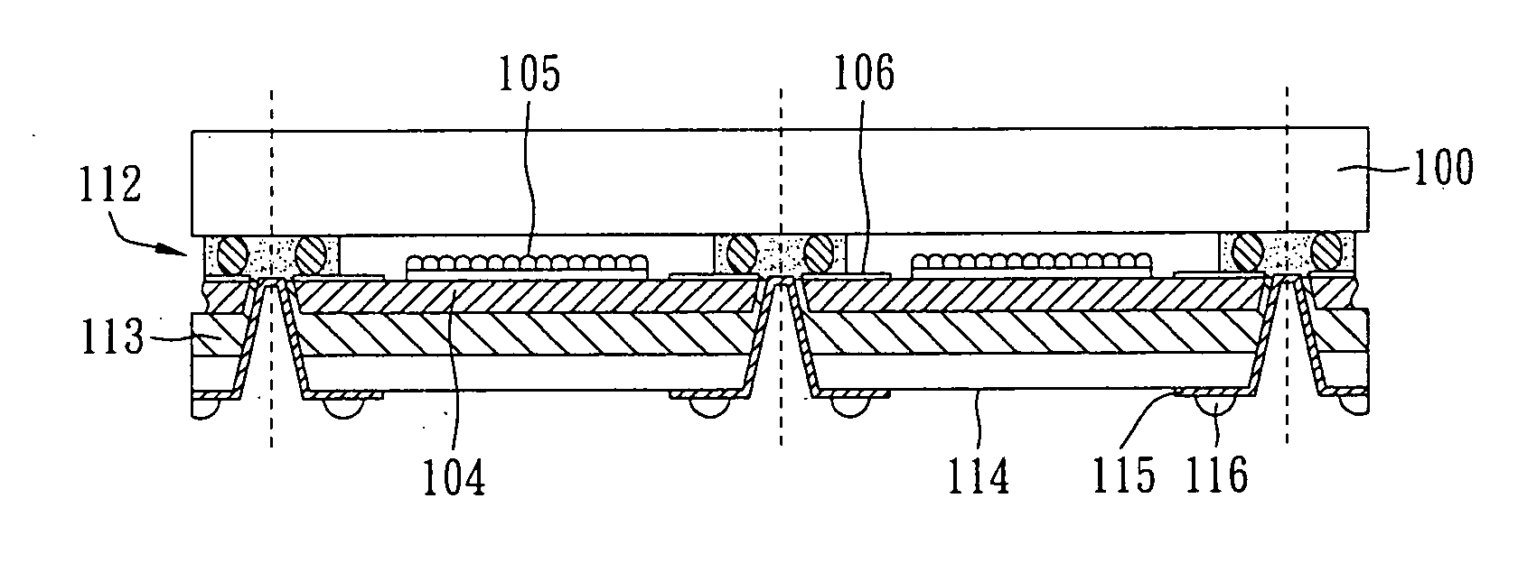
[0026] FIGS. 3(A)-(C) are cross-sectional views of a preferred embodiment according to the present invention, showing a WLCSP process for making a packaged optoelectronic device chip, such as an image sensor chip. Referring to FIG. 3(A), a device substrate 104 is provided, on which optoelectronic devices 105 such as image sensors have been made. A plurality of conductive pads 106 are provided adjacent to the devices 105. The size of the conductive pads may be designed according to circuit or process requirements. The devices 105 and the conductive pads 106 may be made onto the substrate by, e.g., a CMOS process. A transparent upper substrate 100, serving as an upper package layer, is placed over the device substrate 104. As shown in the drawing, there are a plu...


PUM


Abstract

An optoelectronic device chip, and a method for making the chip, are disclosed. The chip comprises a device substrate, an optically transparent upper substrate, and a composite spacer layer which includes an adhesive material and a plurality of particles dispersed in said adhesive material. The distance between the device substrate and the upper substrate is controlled by the thickness of the composite spacer layer so that the variation is within the depth of focus of optical system.

Description

BACKGROUND OF THE INVENTION [0001] 1. Field of the Invention [0002] This invention relates to an optoelectronic device chip. More particularly, this invention relates to an optoelectronic device chip having a composite spacer structure, and a method for making the optoelectronic device chip having the composite spacer structure. [0003] 2. Description of the Related Art [0004] Digital imaging devices have been widely used in many electronic products nowadays. They are used in, for example, digital cameras, digital video recorders, cellular phones with photographing function, safety-control monitors, etc. [0005] A digital imaging device usually includes an optoelectronic device chip, such as a CCD image sensor chip or a CMOS image sensor chip. Such image sensor chips may be packaged by means of an advanced package technology called “wafer-level chip scale package”, WLCSP. In traditional package technology, a wafer having micro-devices such as electronic devices, electromechanical devi...

Claims


Application Information

Patent Timeline
IPC IPC(8): H01L33/00
CPCH01L21/76898H01L23/481H01L27/14618H01L27/14683H01L2223/6622H01L2924/07811H01L2224/274H01L2924/01079H01L2924/00
Inventor LEE, HSIAO-WENZUNG, PETERLIN, TZU-HANLIN, TZY-YINGCHANG, CHIA-YANGLIN, CHIEN-PANG
Owner TAIWAN SEMICON MFG CO LTD
Why Eureka
Try Eureka