Lateral DMOS structure

Inactive Publication Date: 2007-12-06
BCD SEMICON MFG
View PDF3 Cites 0 Cited by
  • Summary
  • Abstract
  • Description
  • Claims
  • Application Information

AI Technical Summary

Benefits of technology

[0004]The primary object of the present invention is to provide a novel lateral DMOS structure that can effectively r

Problems solved by technology

For a DMOS device, the high electric field near the gate results in high surface electron concentration caused by impact ionization.
This phenomenon affects SOA size and device long

Method used


Image

  • Lateral DMOS structure
  • Lateral DMOS structure
  • Lateral DMOS structure

Examples


Example

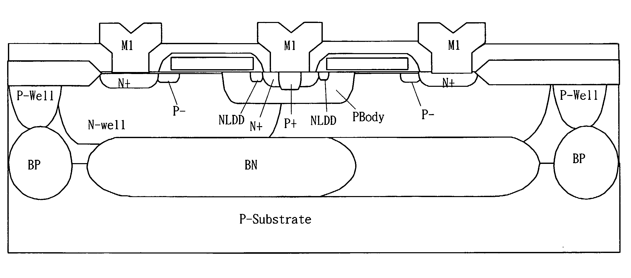
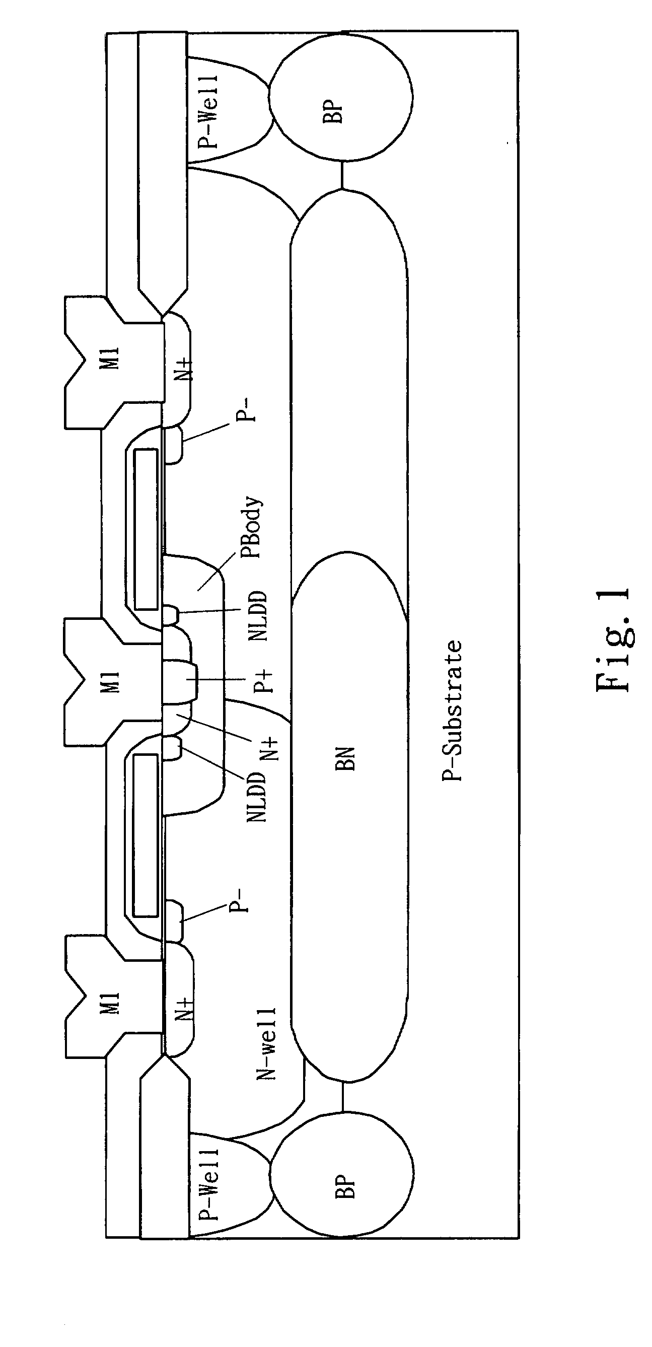
[0018]The present invention aims to provide a lateral DMOS structure that has a light doped p-type region beneath and near the gate at the drain side. Refer to FIG. 1 for the cross section of an embodiment of the invention. It shows that a light doped p-type region (P−) is formed beneath and near the gate at the drain side.

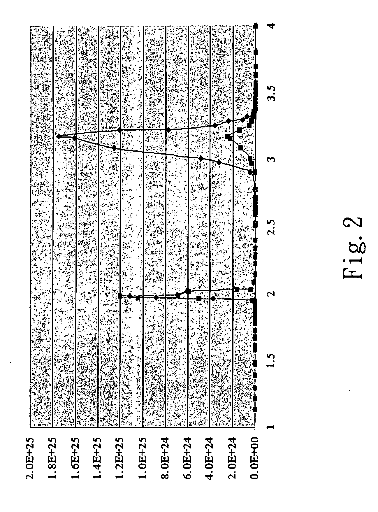
[0019]Because of the existing of the light doped p-type region (P−), the electric field on the surface near the gate is reduced. Refer to FIG. 2 for the comparison of electron impact ionization rate of the lateral DMOS of the invention on the surface near the gate and a conventional DMOS near the gate. The line formed by linking the hollow dots illustrates the distribution of the electron impact ionization rate of the conventional structure. The region around 3 μm corresponds to the gate region. As indicated in the embodiment shown in FIG. 2, the electron impact ionization rate of the conventional DMOS on the surface near the gate is 1.8 E+25. When the lateral DMO...


PUM


Abstract

A lateral DMOS structure includes a light doped p-type region beneath and near the gate at the drain side. The electric field on the surface near the gate is reduced. Thus the electric field near the gate decreases, and the SOA (safe operating area) of the lateral DMOS device increases and long time reliability improves. Moreover, the lateral DMOS of the invention can be fabricated without increasing the manufacturing cost.

Description

FIELD OF THE INVENTION[0001]The present invention relates to an electronic device and a semiconductor manufacturing process thereof and particularly to a lateral DMOS structure.BACKGROUND OF THE INVENTION[0002]In DMOS devices, especially the DMOS devices produced through a semiconductor manufacturing process, the size of SOA (Safe Operating Area) and device long time reliability are two important performance parameters. For a DMOS device, the high electric field near the gate results in high surface electron concentration caused by impact ionization. This phenomenon affects SOA size and device long time reliability.[0003]Hence how to effectively reduce and control the amount of electric field near the gate directly affects SOA size and device long time reliability of the DMOS device.SUMMARY OF THE INVENTION[0004]The primary object of the present invention is to provide a novel lateral DMOS structure that can effectively reduce the electric field near the gate to increase SOA size an...

Claims


Application Information

Patent Timeline
IPC IPC(8): H01L29/78
CPCH01L29/086H01L29/0878H01L29/0619H01L29/7816H01L29/66689
Inventor LIU, XIAN-FENGREN, CHONGHUANG, HAI-TAO
Owner BCD SEMICON MFG
Why Eureka
Try Eureka