Light-emitting element, manufacturing method thereof, light-emitting device, and electronic device

Inactive Publication Date: 2007-12-06
SEMICON ENERGY LAB CO LTD
View PDF18 Cites 4 Cited by
  • Summary
  • Abstract
  • Description
  • Claims
  • Application Information

AI Technical Summary

Benefits of technology

[0010]In view of the foregoing problem, it is an object of the present invention to provide a manufacturing method of a light-emitting element which emits light that has a plurality of emission wavelength peaks. In addition, it is an object of the present invention to provide a light-emitting device and electronic device with high color rendering.
[0022]In addition, in the light-emitting device and electronic device of the present invention, because light is emitted at a plurality of emission wavelength peaks in each, a light-emitting device and an electronic device with high color rendering can be obtained.

Problems solved by technology

However, when light-emitting materials manufactured by these kinds of manufacturing methods are used for thin film inorganic EL elements, a problem arises in which emission of light that has a plurality of emission wavelength peaks is difficult to obtain.

Method used


Image

  • Light-emitting element, manufacturing method thereof, light-emitting device, and electronic device
  • Light-emitting element, manufacturing method thereof, light-emitting device, and electronic device
  • Light-emitting element, manufacturing method thereof, light-emitting device, and electronic device

Examples


embodiment mode 1

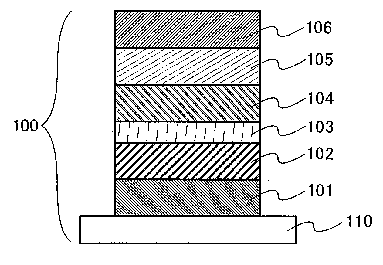
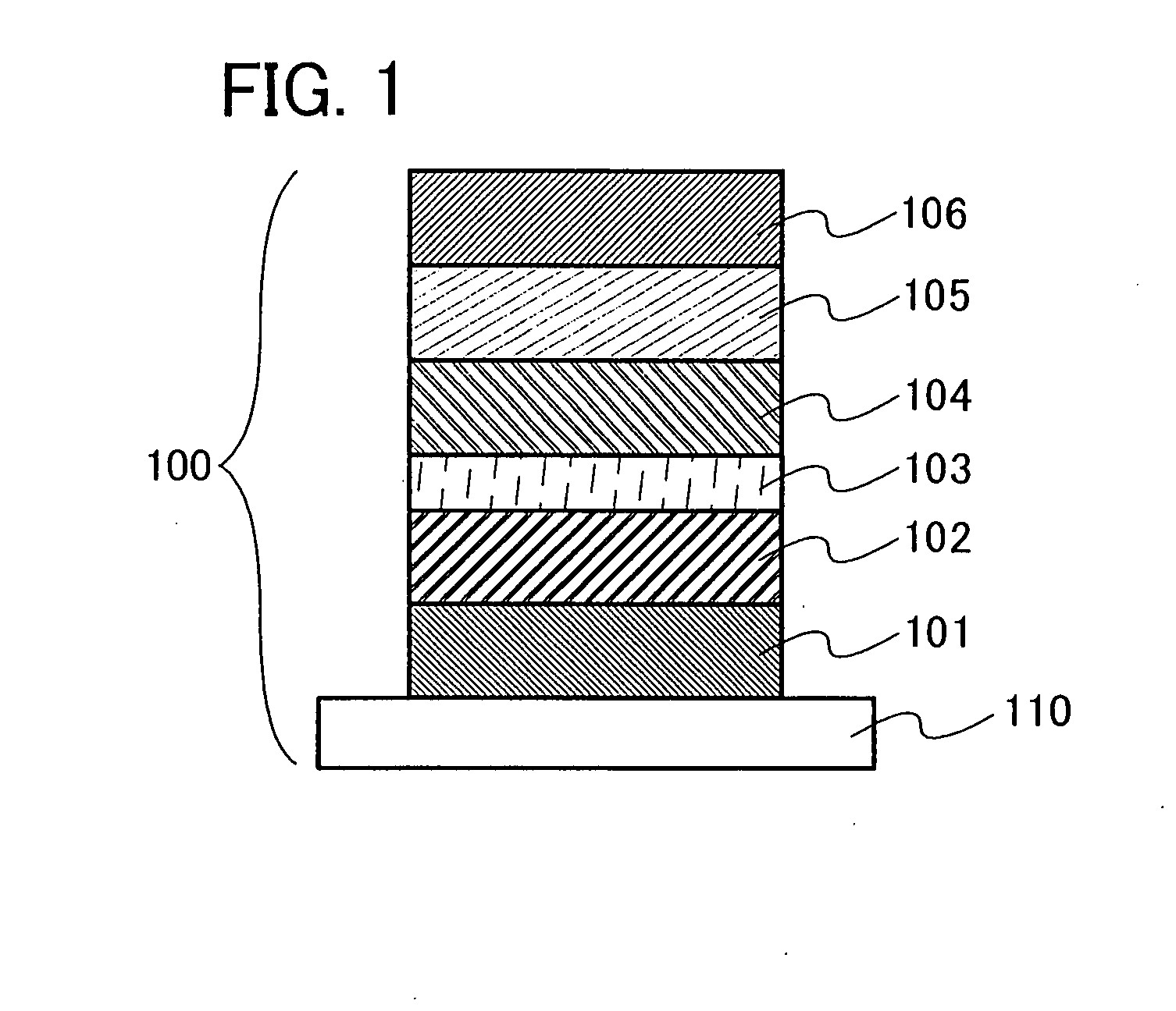
[0038]In the present embodiment mode, a manufacturing method for a thin film light-emitting element of the present invention will be explained using FIG. 1.

[0039]In FIG. 1, a thin film element 100 with a light-emitting layer includes, over a substrate 110, a first electrode 101 and a second electrode 106; a first insulating layer 102 and a second insulating layer 105 that are in contact with the first electrode 101 and the second electrode 106, respectively; and a first layer 103 and a second layer 104 formed between the first insulating layer 102 and second insulating layer 105. In the present embodiment mode, a manufacturing method for a light-emitting element in which, after thin film formation, heat treatment is performed, whereby emission of light from a light-emitting layer is obtained, will be explained hereinafter.

[0040]The substrate 110 is used as a base for a light-emitting element. For the substrate 110, for example, glass, quartz, plastic, or the like can be used. It is ...

embodiment mode 2

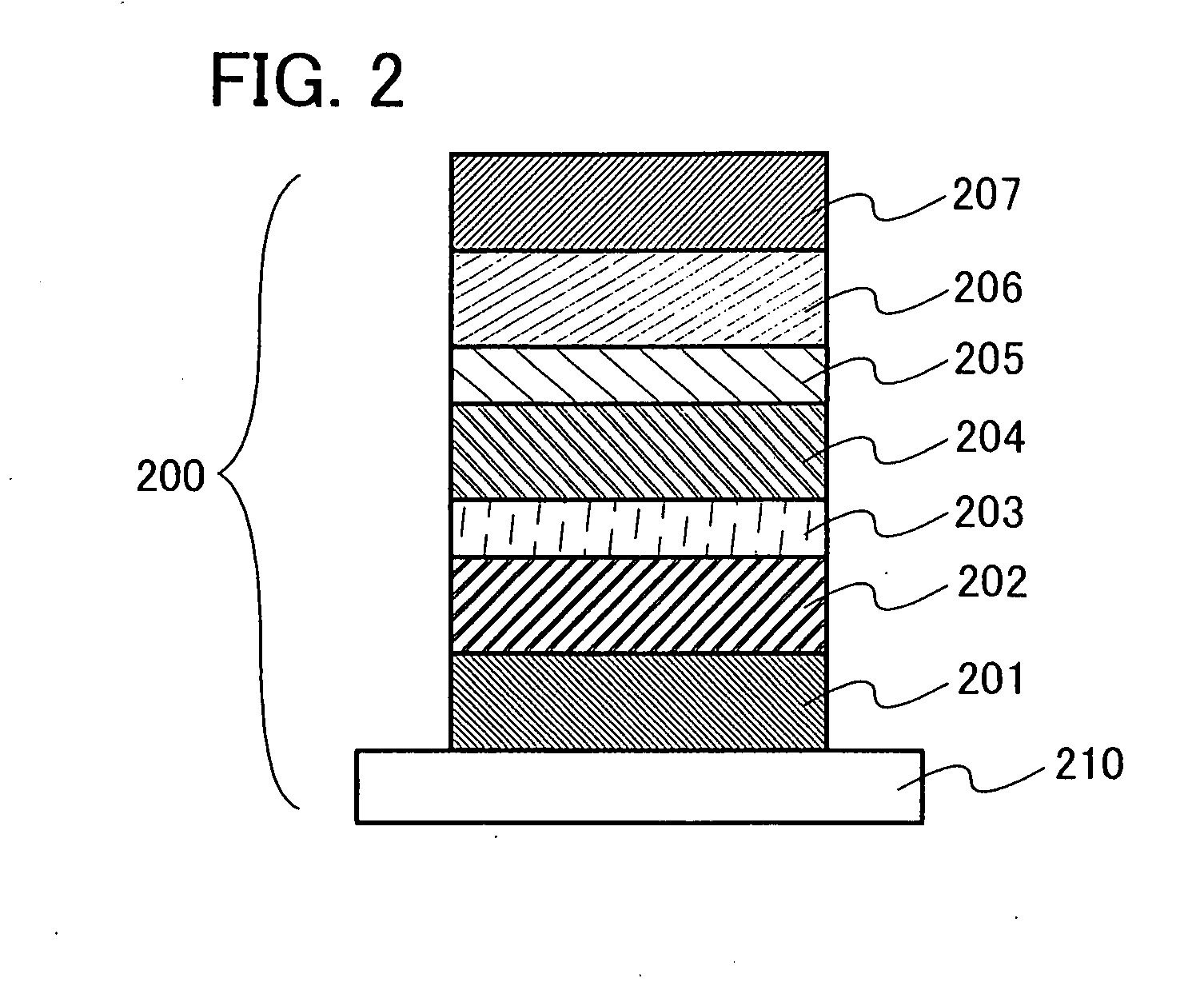
[0049]In the present embodiment mode, a thin film light-emitting element of the present invention will be described using FIG. 2.

[0050]In FIG. 2, a thin film element 200 with a light-emitting layer includes, over a substrate 210, a first electrode 201 and a second electrode 207; a first insulating layer 202 and a second insulating layer 206 that are in contact with the first electrode 201 and the second electrode 207, respectively; and a first layer 203, a second layer 204, and a third layer 205 formed between the first insulating layer 202 and the second insulating layer 206. As in Embodiment Mode 1, a manufacturing method of a light-emitting element in which, after thin film formation, heat treatment is performed, whereby emission of light from a light-emitting layer is obtained, will be explained hereinafter.

[0051]For the substrate 210, the first electrode 201 and second electrode 207, and the first insulating layer 202 and second insulating layer 206, the materials described in ...

embodiment mode 3

[0057]In the present embodiment mode, a thin film light-emitting element of the present invention will be explained using FIG. 3.

[0058]In FIG. 3, a thin film element 300 includes a first electrode 301 and a second electrode 309, a first insulating layer 302 and a second insulating layer 308 that are in contact with the first electrode 301 and the second electrode 309, respectively; and a first layer 303, a second layer 304, a third layer 305, a fourth layer 306, and a fifth layer 307 formed between the first insulating layer 302 and the second insulating layer 308, all formed over a substrate 310. As in Embodiment Mode 1, a manufacturing method of a light-emitting element in which, after thin film formation, heat treatment is performed whereby emission of light from a plurality of layers containing host materials which a light-emitting layer includes is obtained, will be explained hereinafter.

[0059]For the substrate 310, the first electrode 301 and second electrode 309, and the firs...


PUM


Abstract

It is an object of the present invention to provide a manufacturing method for a light-emitting element that emits light at a plurality of emission wavelength peaks. Furthermore, it is an object of the present invention to provide a light-emitting device and electronic device in which color rendering is high. A manufacturing method for a light-emitting element includes the following steps: a step for forming a first electrode, a step for forming a light-emitting layer over the first electrode, a step for forming a second electrode over the light-emitting layer, and a step for performing heat treatment on the light-emitting layer; where the step for forming the light-emitting layer includes a step for forming a layer containing a host material and a layer containing a material acting as a luminescent center so that the two layers are in contact with each other.

Description

BACKGROUND OF THE INVENTION[0001]1. Field of the Invention[0002]The present invention relates to a light-emitting element that uses electroluminescence. In addition, the present invention relates to a light-emitting device and electronic device that each have a light-emitting element.[0003]2. Description of the Related Art[0004]In recent years, for display units in televisions, cellular telephones, digital cameras, and the like, planar and thin display units have been demanded, and for a display unit that meets this demand, display units that use self-emitting light-emitting elements have been attracting attention. For one kind of self-emitting light-emitting element, there is a light-emitting element that uses electroluminescence; emission of light from a light-emitting material can be obtained by application of a voltage to a light-emitting element where a light-emitting material is interposed between a pair of electrodes.[0005]For this kind of self-emitting light-emitting element...

Claims


Application Information

Patent Timeline
IPC IPC(8): H01J1/62H01J63/04
CPCC09K11/574H05B33/14C09K11/612H05B33/20
Inventor SAKATA, JUNICHIRO
Owner SEMICON ENERGY LAB CO LTD
Why Eureka
Try Eureka