Method of compensating for channel interference of display apparatus and device for controlling driving of data signal

a technology of display apparatus and data signal, which is applied in the direction of electric digital data processing, instruments, computing, etc., can solve the problems of inability to compensate the interference phenomenon caused by connection wires on the panel, the current cannot rapidly reach a sufficient signal level within a predetermined driving time, and the offset voltage has to be designed to be extremely minute, so as to achieve the effect of compensating for a luminance chang

Inactive Publication Date: 2007-12-06
HANA MICRON
View PDF3 Cites 14 Cited by
  • Summary
  • Abstract
  • Description
  • Claims
  • Application Information

AI Technical Summary

Benefits of technology

[0026]The present invention provides a method of compensating for channel interference of a display apparatus capable of effectively compensating for a luminance change caused by the channel interference phenomenon which may occur when a display panel is driven.

Problems solved by technology

On the other hand, in the OLED display apparatus, since each pixel has a parasitic capacitance, even when the driving current is supplied, the driving current cannot rapidly reach a sufficient signal level within a predetermined driving time.
The interference phenomenon caused by connection wires on the panel cannot be compensated for.
However, in order to embody the aforementioned OP-AMP, an offset voltage has to be designed to be extremely minute.
Therefore, a size and power consumption of the driving IC increase.

Method used


Image

  • Method of compensating for channel interference of display apparatus and device for controlling driving of data signal
  • Method of compensating for channel interference of display apparatus and device for controlling driving of data signal
  • Method of compensating for channel interference of display apparatus and device for controlling driving of data signal

Examples


Embodiment Construction

[0043]Now, preferred embodiments of the present invention will be described in detail with reference to the attached drawings. In addition, in order to clearly describe exemplary embodiments with reference to the accompanying drawings, specific technical terms are used. However, the present invention is not limited to the selected specific technical terms, and each specific technical term includes all the technical synonyms which operate in a similar manner so as to achieve a similar object.

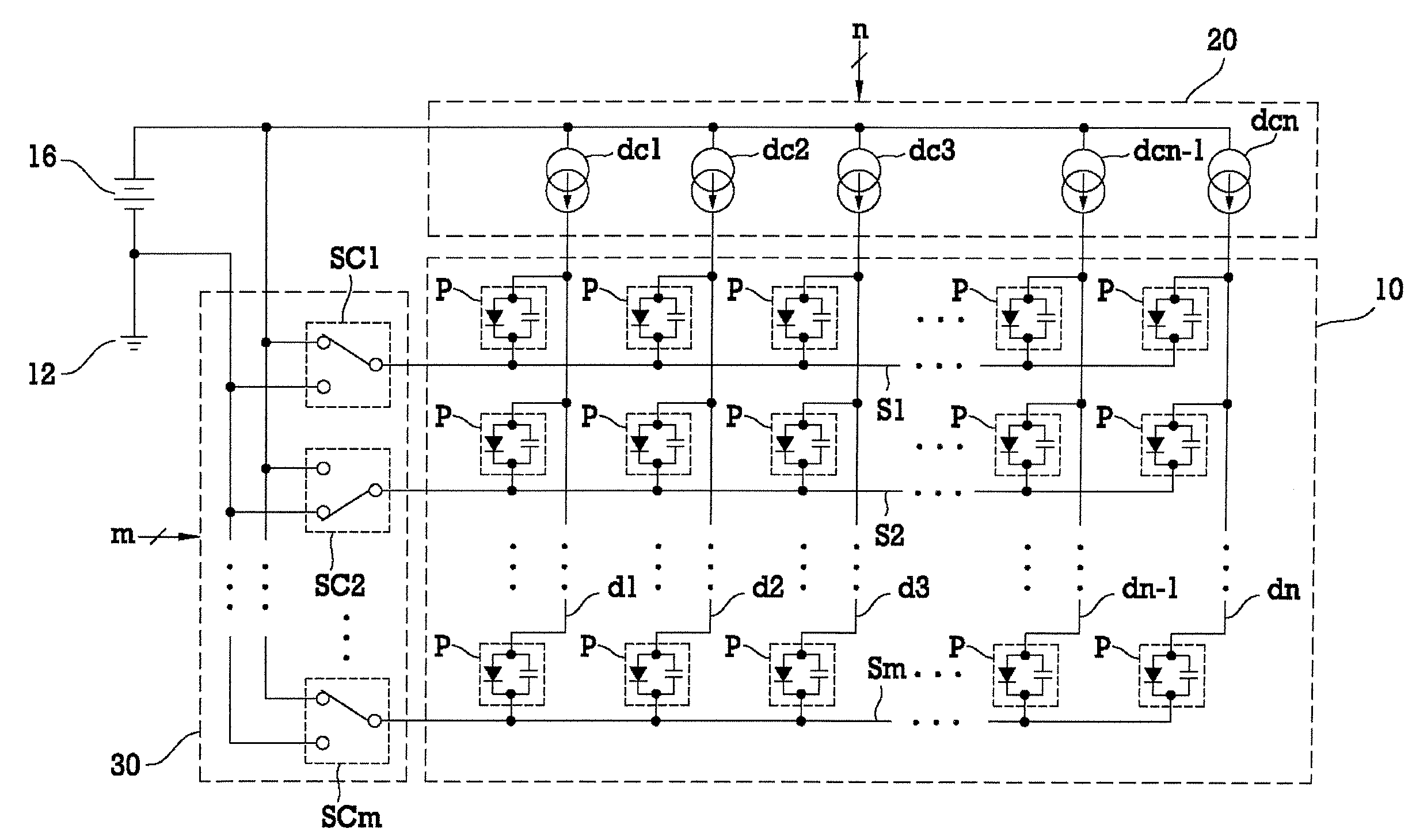
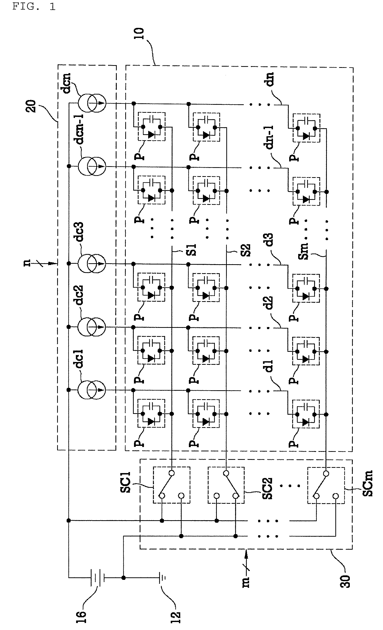
[0044]FIG. 4 is a circuit diagram illustrating a display apparatus including a device for controlling driving of a data signal according to an exemplary embodiment of the present invention. FIG. 4 illustrates a passive matrix OLED display apparatus which includes the device for controlling driving of a data signal.

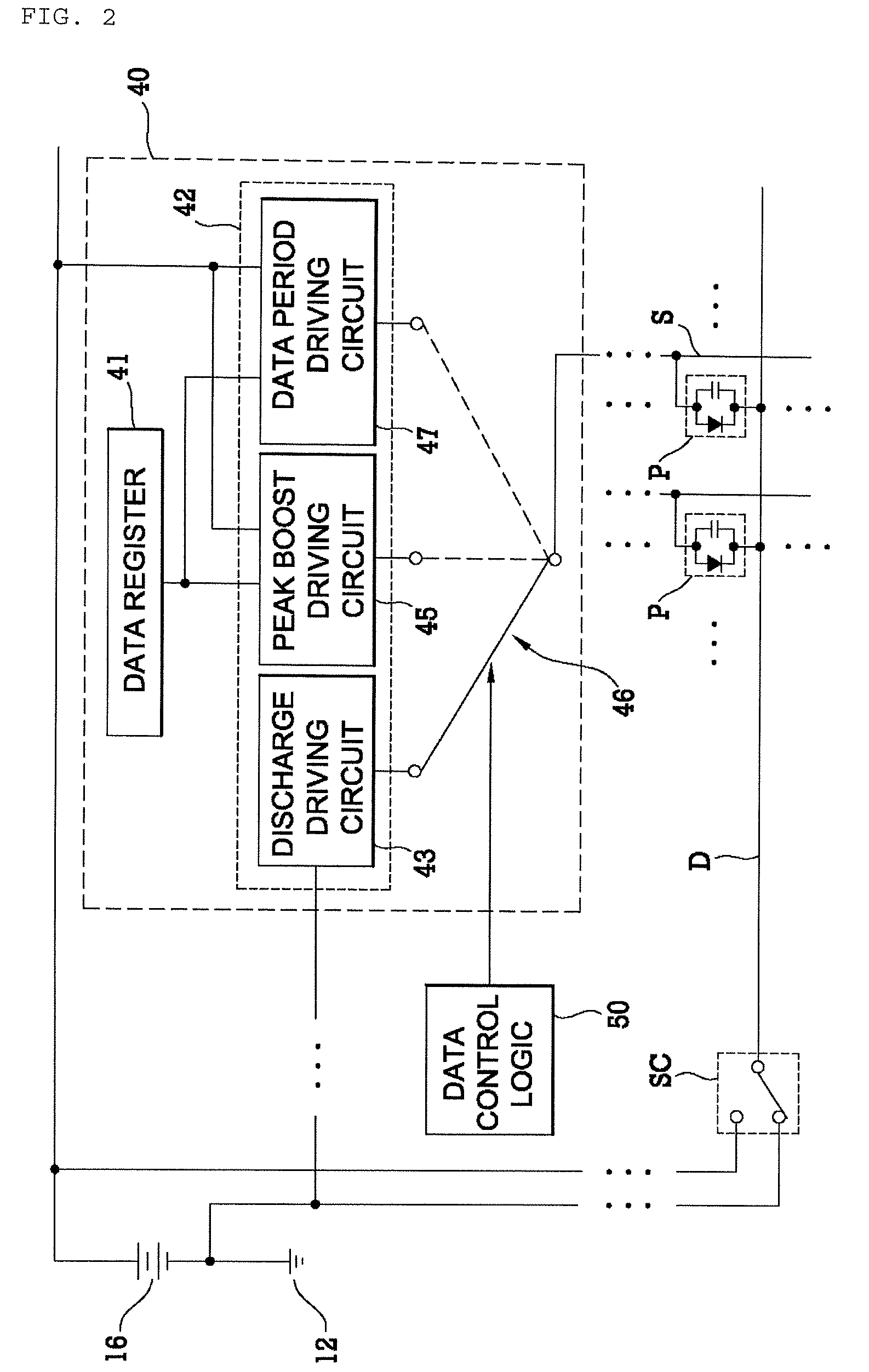
[0045]As shown in FIG. 4, the OLED display apparatus may include a screen memory 200. In the screen memory 200, pixel data according to a frame screen to be displayed is stored for each...


PUM


Abstract

A method of compensating for channel interference of a display apparatus and a device for controlling driving of a data signal are provided. The method of compensating for the channel interference of the display apparatus includes: receiving pixel data of a scan line selected from an external screen memory; summing up the received pixel data and detecting a compensation time for compensating for channel interference which occurs in the selected scan line by using the sum of the pixel data; and adjusting at least one of a discharge time and a peak boost time of a driving current that is output to each data line according to the detected compensation time. Accordingly, it is possible to solve problems such as an increase of the circuit size caused by the existing compensation for the channel interference by controlling the discharge period or peak boost period with respect to each scan line and compensating for the channel interference phenomenon.

Description

BACKGROUND[0001]1. Technical Field[0002]The present invention relates to a method of compensating for channel interference of a display apparatus and a method of controlling driving of a data signal, and more particularly, to a method of compensating for channel interference of a display apparatus in which a channel interference phenomenon that occurs when a display panel is driven by controlling a time length of a discharge period or peak boost period for each scan line and a device for controlling driving of a data signal related thereto.[0003]2. Related Art[0004]Recently, a light emitting device using an emissive element and a light emitting display apparatus employing the light emitting device as a pixel have been actively developed. At this time, the emissive element may have various shapes by using various materials such as an organic material, a non-organic material, a thin film material, a bulk material, a distributed material, and the like.[0005]One of the typical emissive ...

Claims


Application Information

Patent Timeline
Patent Type & Authority Applications(United States)
IPC IPC(8): G09G3/20
CPCG09G3/3216G09G3/3283G09G2310/0248G09G2360/16G09G2310/08G09G2320/0223G09G2310/0251G09G3/20G09G3/30
Inventor PARK, JINLEE, JOON-SEOKJUNG, DAE YOUNG
Owner HANA MICRON
Why Eureka
Try Eureka