Self aligned gate JFET structure and method

Inactive Publication Date: 2007-12-13
MIE FUJITSU SEMICON
View PDF3 Cites 65 Cited by
  • Summary
  • Abstract
  • Description
  • Claims
  • Application Information

AI Technical Summary

Benefits of technology

[0016]The genus of processes according to the teachings of the invention result in a JFET being constructed which has a self-aligned gate contact. This is achieved by forming the gate contact from a second polysilicon layer (although the first layer from which the source and drain contacts are made may not be polysilicon and can be some other conductor) which is deposited into an opening formed by formation of spacer oxide around the source an

Problems solved by technology

A nitride layer covering the field oxide prevents o

Method used


Image

  • Self aligned gate JFET structure and method
  • Self aligned gate JFET structure and method
  • Self aligned gate JFET structure and method

Examples


Embodiment Construction

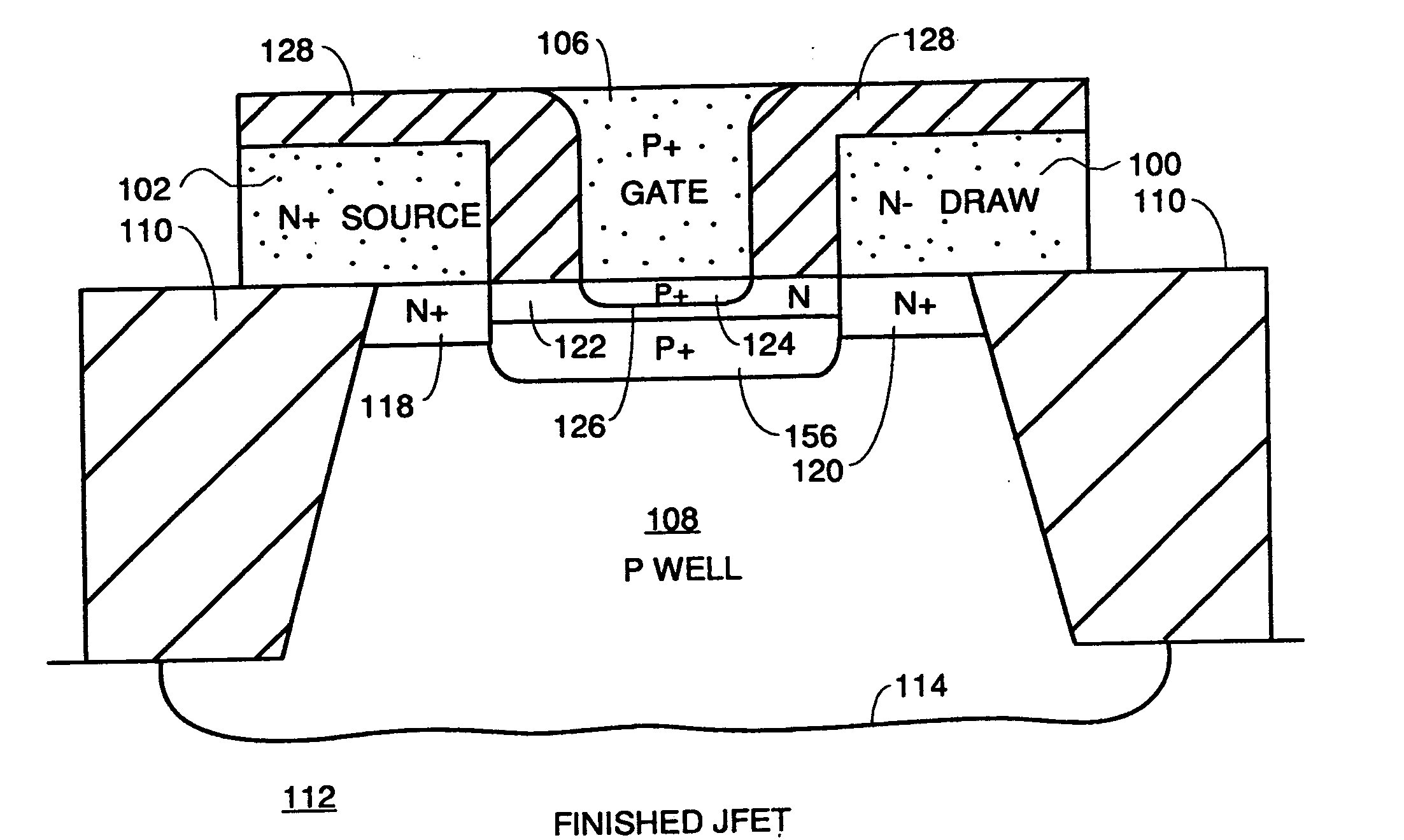
[0045]FIG. 5A is a plan view of the finished JFET according to one embodiment of the invention. Source contact 100 is preferably made from first polysilicon (hereafter poly), but it may also be made from some refractory metal or silicide or a combination of polysilicon, silicide and refractory metal. The same is true for drain contact 102. An insulating spacer 128 called spacer dielectric structures in the claims, typically silicon dioxide, separates the drain and source contacts from a self-aligned gate contact 106 made from “second” poly (second poly means whatever doped semiconductor or conductor is used to form the gate contact and does not require that the source and drain contacts be formed of first poly).

[0046]Spacer dielectric structure 128 may also be comprised of multiple layers of dielectric material such as silicon dioxide and silicon nitride (Si3N4), and the term should be so interpreted in the claims. Box 108 represents the active area in the substrate which is electri...


PUM


Abstract

A JFET integrated onto a substrate having a semiconductor layer at least and having source and drain contacts over an active area and made of first polysilicon (or other conductors such as refractive metal or silicide) and a self-aligned gate contact made of second polysilicon which has been polished back to be flush with a top surface of a dielectric layer covering the tops of the source and drain contacts. The dielectric layer preferably has a nitride cap to act as a polish stop. In some embodiments, nitride covers the entire dielectric layer covering the source and drain contacts as well as the field oxide region defining an active area for said JFET. An embodiment with an epitaxially grown channel region formed on the surface of the substrate is also disclosed.

Description

BACKGROUND OF THE INVENTION[0001]The invention pertains to a device structure and method for making JFET transistors at very small line widths which can overcome certain process problems in CMOS circuits built with small line widths.[0002]As line widths have shrunk steadily down into the submicron range (today's line widths are 45 nanometers or 0.045 microns where a micron is 10−6 meters and one nanometer equals 10 angstroms), all structures on CMOS, NMOS and PMOS circuits have shrunk including the thickness of the gate oxide. As line widths shrink, the voltages must be dropped to avoid punch through. This shrinking line width means smaller gate length which requires that the thickness of gate oxide must also be reduced to allow proper control of the current flow in MOS devices at the lower voltages. Reduced gate oxide thickness results in increased gate capacitance per unit area which has to be switched. Since smaller geometries imply increased circuit density, the result is an ove...

Claims


Application Information

Patent Timeline
IPC IPC(8): H01L31/112
CPCH01L29/1066H01L29/808H01L29/66901H01L29/41775H01L29/66893
Inventor KAPOOR, ASHOK KUMAR
Owner MIE FUJITSU SEMICON
Why Eureka
Try Eureka