
Display substrate and display device having the same

a display substrate and substrate technology, applied in the field of display substrates, can solve problems such as adversely affecting image display quality, and achieve the effects of improving image display quality, increasing the uniformity of line resistance, and reducing the reaction of the fan-out par

Inactive Publication Date: 2007-12-27
SAMSUNG DISPLAY CO LTD
View PDF3 Cites 24 Cited by
  • Summary
  • Abstract
  • Description
  • Claims
  • Application Information

AI Technical Summary

Benefits of technology

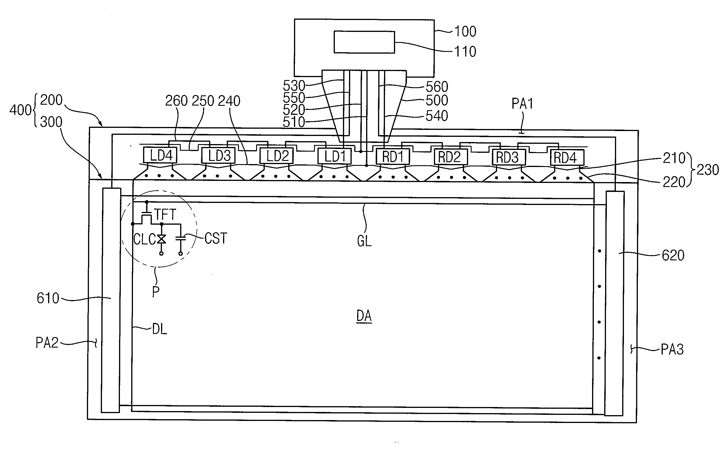
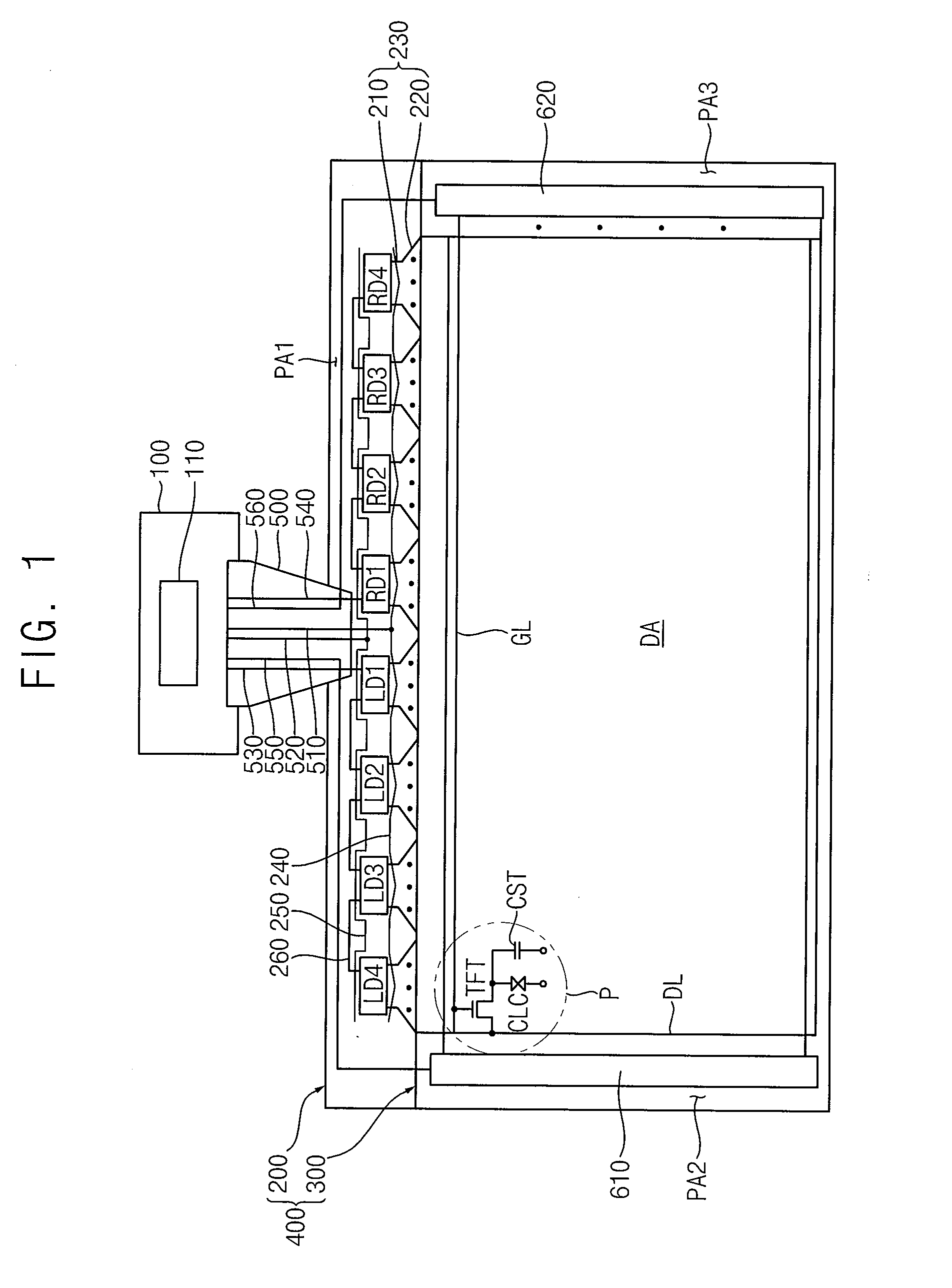
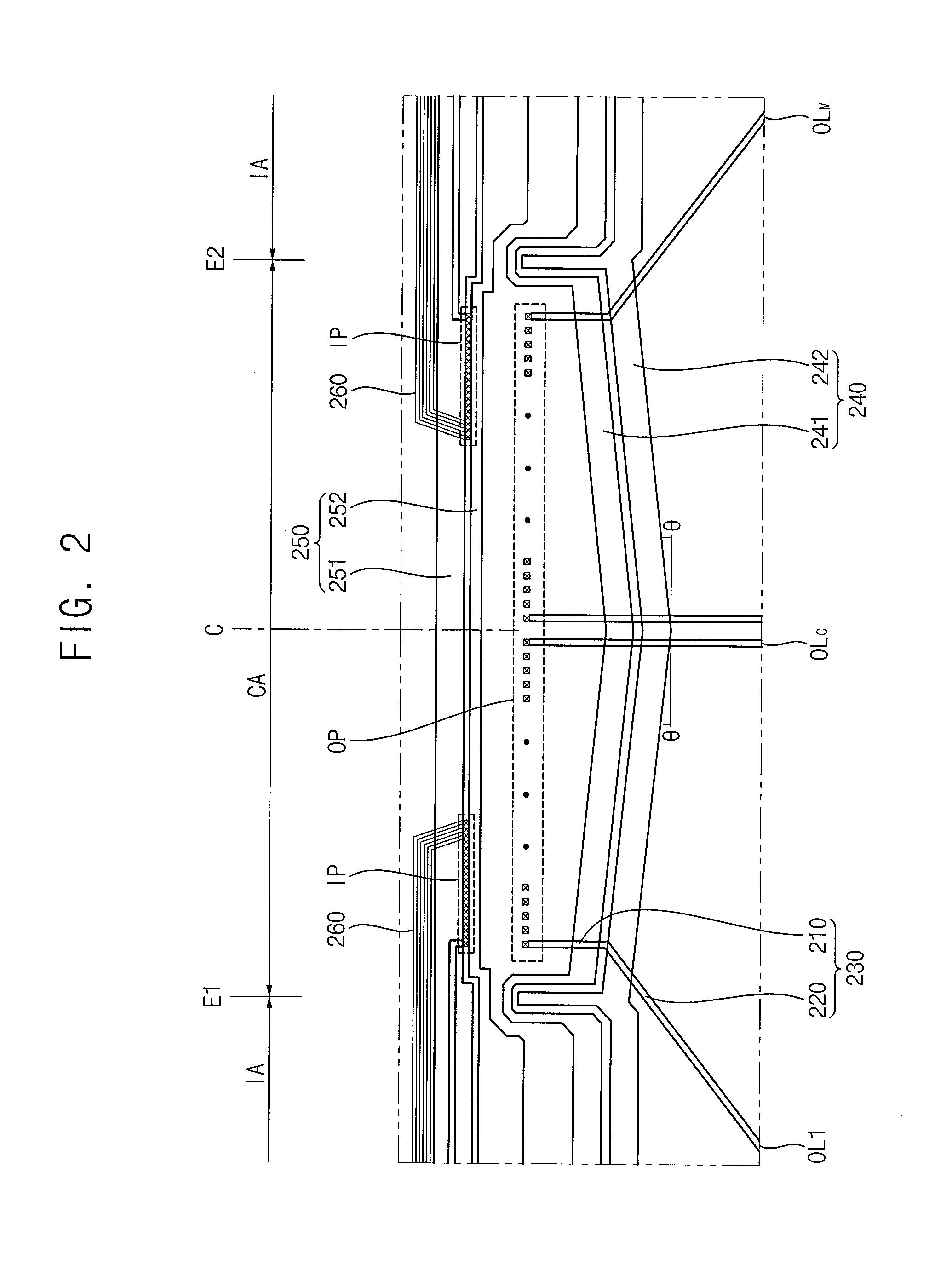
[0007]A display substrate in accordance with another embodiment of the present invention includes a plurality of source lines, a plurality of gate lines, a driving chip, a first voltage line and a fan-out part. The source lines are disposed in a display area. The gate lines are disposed in the display area, and insulatingly crossing the source lines. The driving chip is disposed in a peripheral area surrounding the display area. The fan-out part has a plurality of output lines electrically connected between the driving chip and the source lines and crossing the first voltage line at angles to minimize capacitive reactance of the output lines.
[0009]According to the present invention, the first voltage line that is directly formed on the display panel is inclined with respect to a horizontal line of the display panel and is partially overlapped by the fan-out part thereby decreasing the line reactance of the fan-out part and increasing the uniformity of line resistance to improve image display quality.

Problems solved by technology

However, this structure increases the line resistance of the metal lines causing an RC delay of the signal, thereby adversely affecting image display quality.

Method used


Image

  • Display substrate and display device having the same
  • Display substrate and display device having the same
  • Display substrate and display device having the same

Examples


Embodiment Construction

[0016]It will be understood that when an element or layer is referred to as being “on,”“connected to” or “coupled to” another element or layer, it can be directly on, connected or coupled to the other element or layer or intervening elements or layers may be present. In contrast, when an element is referred to as being “directly on,”“directly connected to” or “directly coupled to” another element or layer, there are no intervening elements or layers present. Like numbers refer to like elements throughout. Embodiments of the invention are described herein with reference to cross-section illustrations that are schematic illustrations of idealized embodiments (and intermediate structures) of the invention. As such, variations from the shapes of the illustrations as a result, for example, of manufacturing techniques and / or tolerances, are to be expected. Thus, the regions illustrated in the figures are schematic in nature and their shapes are not intended to illustrate the actual shape ...


PUM


Abstract

A display substrate includes source lines, gate lines, an output pad part, a fan-out part and a first voltage line part. The source lines are in a display area. The gate lines cross the source lines. The output pad part is in a peripheral area surrounding the display area and is electrically connected to output terminals of a driving chip. The fan-out part is electrically connected between the output pad part and the source lines. The first voltage line part is inclined with respect to a central line of a chip area in which the driving chip is mounted toward opposite sides of the chip area to cross the fan-out part. Therefore, the line reactance of the fan-out part is decreased and the uniformity of the line resistance of the fan-out part is increased to improve image display quality.

Description

CROSS-REFERENCE TO RELATED APPLICATIONS[0001]The present application claims priority from Korean Patent Application No. 2006-57796, filed on Jun. 27, 2006, the disclosure of which is hereby incorporated herein by reference.FIELD OF THE INVENTION[0002]The present invention relates to a display device having and, more particularly, to a display device having a substrate with more uniform line resistance.DESCRIPTION OF THE RELATED ART [0003]A liquid crystal display (LCD) device, in general, includes a display panel, a gate driving circuit and a source driving circuit. The display panel displays an image by varying the light transmittance of the liquid crystal molecules. The gate driving circuit is electrically connected to the display panel to generate a gate signal. The data driving circuit is electrically connected to the display panel to generate a data signal. The display panel includes a plurality of pixel parts. Each of the pixel parts includes a switching element and a liquid cr...

Claims


Application Information

Patent Timeline
IPC IPC(8): G09G3/36
CPCG02F1/13452G02F1/1345
Inventor KWAK, YUN-HEEMOON, SEUNG-HWANCHANG, JONG-WOONG
Owner SAMSUNG DISPLAY CO LTD
Learn More