Method and its apparatus for inspecting a pattern

a pattern and pattern technology, applied in the direction of semiconductor/solid-state device testing/measurement, image enhancement, instruments, etc., can solve the problems of incorrect inspection in such a changed state of the object, judging to be a defect, and affecting the inspection accuracy

Inactive Publication Date: 2008-01-03
HIROI TAKASHI +7
View PDF13 Cites 16 Cited by
  • Summary
  • Abstract
  • Description
  • Claims
  • Application Information

AI Technical Summary

Problems solved by technology

If a difference from the reference image is recognized in an image-acquired area, it is judged to be a defect.
In the case of a SEM type inspection apparatus, if inspection is conducted plural times, irradiation of the electron beam is carried out plural times, with the result that the state of the object changes due to electron beam irradiation and the inspection is inaccurate in such a changed state of the object.
If the pattern density differs, the amplitude in detected signal quantity of a detected pattern differs because there is a limit in the resolution of the inspection system.
Therefore, even in the case of defects of the same size, if inspection is performed with uniform sensitivity, there arise both a detected place and an undetected place because of different background patterns.
Moreover, even defects of the same size differ in point of whether they can be critical or not.
Conversely, a place high in pattern density can be a critical defect even if it is a minute defect.
It is impossible to consider detection sensitivity, defect management and design information separately from one another.
However, a wafer pattern for a semiconductor device is constituted by a very complicated pattern, so by utilizing a mere simple regularity, it is impossible to set an area not to be inspected, nor is it possible to obtain plural inspection results in a single inspection.
But since this area not to be inspected, or a non-inspection area, is limited to pattern edges, it is impossible to set a non-inspection area at a required place, nor is it possible to obtain plural inspection results in a single inspection.
Besides, plural inspection results cannot be obtained in a single inspection.

Method used


Image

  • Method and its apparatus for inspecting a pattern
  • Method and its apparatus for inspecting a pattern
  • Method and its apparatus for inspecting a pattern

Examples


first embodiment

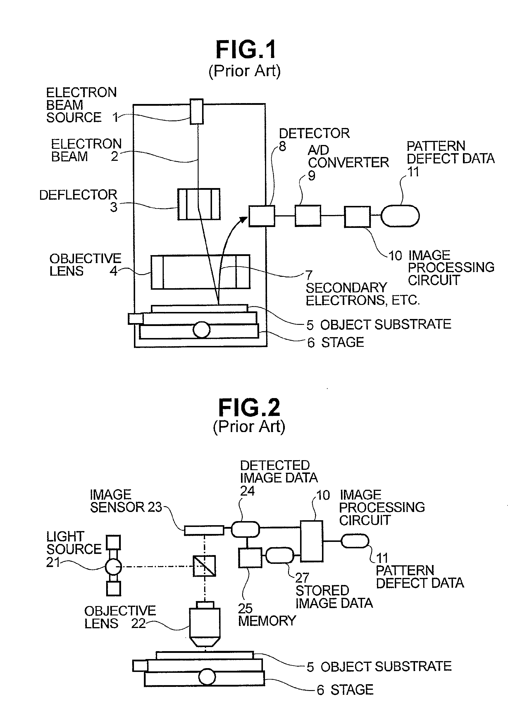
[0058] A first embodiment of the present invention will be described with reference to FIG. 6, which illustrates an example of the configuration of an electron beam type pattern inspecting apparatus according to the invention.

[0059] The electron beam type pattern inspecting apparatus is composed of an electron beam source 1 having an electron gun for emitting an electron beam 2, and an electron optical system which extracts the electron beam 2 from the electron beam source 1 while accelerating it and which forms a virtual light source at a certain position using an electrostatic or electromagnetic lens. The electron optical system comprises a condenser lens 103 for converging the electron beam 2 from the virtual light source to a certain position, a blanking plate 63 installed near a position where the electron beam is converged by the electron gun to effect ON / OFF of the electron beam 2, a deflector 105 for deflecting the electron beam 2 in XY directions, and an objective lens 4 f...

second embodiment

[0112] A second embodiment of the present invention will be described with reference to FIG. 16, which shows an example of the configuration of the second embodiment.

[0113] A pattern inspecting apparatus according to this second embodiment is made up of an electron beam source 1 having an electron gun for emitting an electron beam 2, and an electron optical system which extracts the electron beam 2 from the electron beam source 1 while accelerating it and which forms a virtual light source at a certain position with use of an electrostatic or electromagnetic lens. The electron optical system comprises a condenser lens 103 for converging the electron beam 2 from the virtual light source to a certain position, a blanking plate 63 installed near a position where the electron beam is converged by the electron gun to effect ON / OF control of the electron beam 2, a deflector 105 for deflecting the electron beam 2 in XY directions, and an objective lens 4 for converging the electron beam 2...

third embodiment

[0130] A third embodiment of the present invention will now be described with reference to FIG. 20, which illustrates an embodiment of the configuration of an electron beam type pattern inspecting apparatus according to the present invention. The electron beam type pattern inspecting apparatus is composed of an electron beam source 1 having an electron gun for emitting an electron beam 2, and an electron optical system which extracts the electron beam 2 from the electron beam source 1 while accelerating it and which forms a virtual light source 101 at a certain position using an electrostatic or electromagnetic lens. The electron optical system comprises a condenser lens 103 for converging the electron beam 2 from the virtual light source to a certain position, a blanking plate 63 installed near a position where the electron beam is converged by the electron gun to effect ON / OFF control of the electron beam 2, a deflector 105 for deflecting the electron beam 2 in XY directions, and ...


PUM

PropertyMeasurementUnit
diameteraaaaaaaaaa
electron beamaaaaaaaaaa
image processingaaaaaaaaaa

Abstract

In a pattern inspecting apparatus, images of places which can be expected to be the same pattern are compared with one another. However, a comparison of images obtained by different stage scans and the occurrence of a place capable of being inspected only once lead to a deterioration in the performance of detecting various error defects and an area incapable of being inspected, respectively. For solving this problem, defects detected in a high sensitivity condition are regarded as defect candidates and a critical threshold value, used as a boundary to detect a smaller value as a defect, of a defect candidate portion is obtained by an image processing circuit or an image of the defect candidate portion is obtained by processing with software. Further, the critical threshold value thus obtained is compared with plural threshold values, thereby permitting plural inspection results to be obtained in a single inspection.

Description

CROSS REFERENCE TO RELATED APPLICATION [0001] This application is a Continuation of U.S. application Ser. No. 10 / 062,632, filed Feb. 5, 2002, which claims prior from Japanese Patent Application No. 2001-207213, filed on Jul. 9, 2001, the contents of which are incorporated herein by reference.BACKGROUND OF THE INVENTION [0002] The present invention relates to an apparatus for fabricating a substrate having a circuit pattern of, for example, a semiconductor device or a liquid crystal display. More particularly, the invention is concerned with a technique for inspecting a pattern on a substrate during manufacture. [0003] Conventional electron beam type and optical type pattern inspecting apparatuses are disclosed in JP-A Nos. 258703 / 1993 and 160247 / 1999, respectively. More particularly, an example of an electron beam type inspection apparatus is disclosed in the JP-A No. 258703 / 1993, the construction of which is shown in FIG. 1. [0004] As seen in FIG. 1, an electron beam 2 emitted from...

Claims


Application Information

Patent Timeline
Patent Type & Authority Applications(United States)
IPC IPC(8): G06K9/00G01N23/00G01N21/956G06T1/00G06T7/00H01J37/22H01L21/66
CPCG06T2207/30148G06T7/001
Inventor HIROI, TAKASHIWATANABE, MASAHIROTANAKA, MAKIKUNI, ASAHIROSHISHIDO, CHIEMIYAI, HIROSHINARA, YASUHIKOISOBE, MITSUNOBU
Owner HIROI TAKASHI
Why Eureka
Try Eureka