Pixel circuit, image display apparatus, driving method therefor and driving method of electronic device
a technology of image display and driving method, which is applied in the direction of static indicating devices, instruments, electroluminescent light sources, etc., can solve the problem of high rate of deterioration of asi-tft, and achieve the effect of reducing the shift amount of a threshold voltag
- Summary
- Abstract
- Description
- Claims
- Application Information
AI Technical Summary
Benefits of technology
Problems solved by technology
Method used
Image
Examples
first embodiment
[0040] An image display apparatus in this embodiment includes a plurality of pixels arranged in a matrix. Each of the pixels has a light emitting element and a driver.
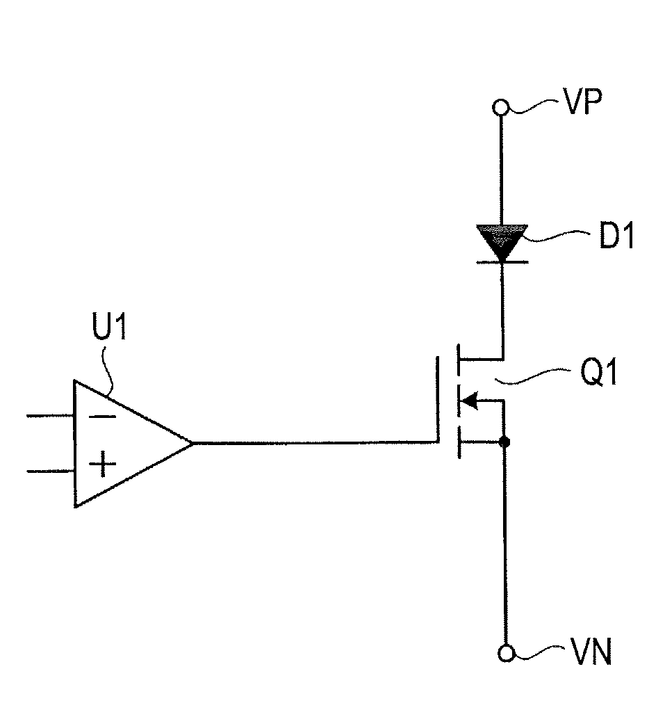
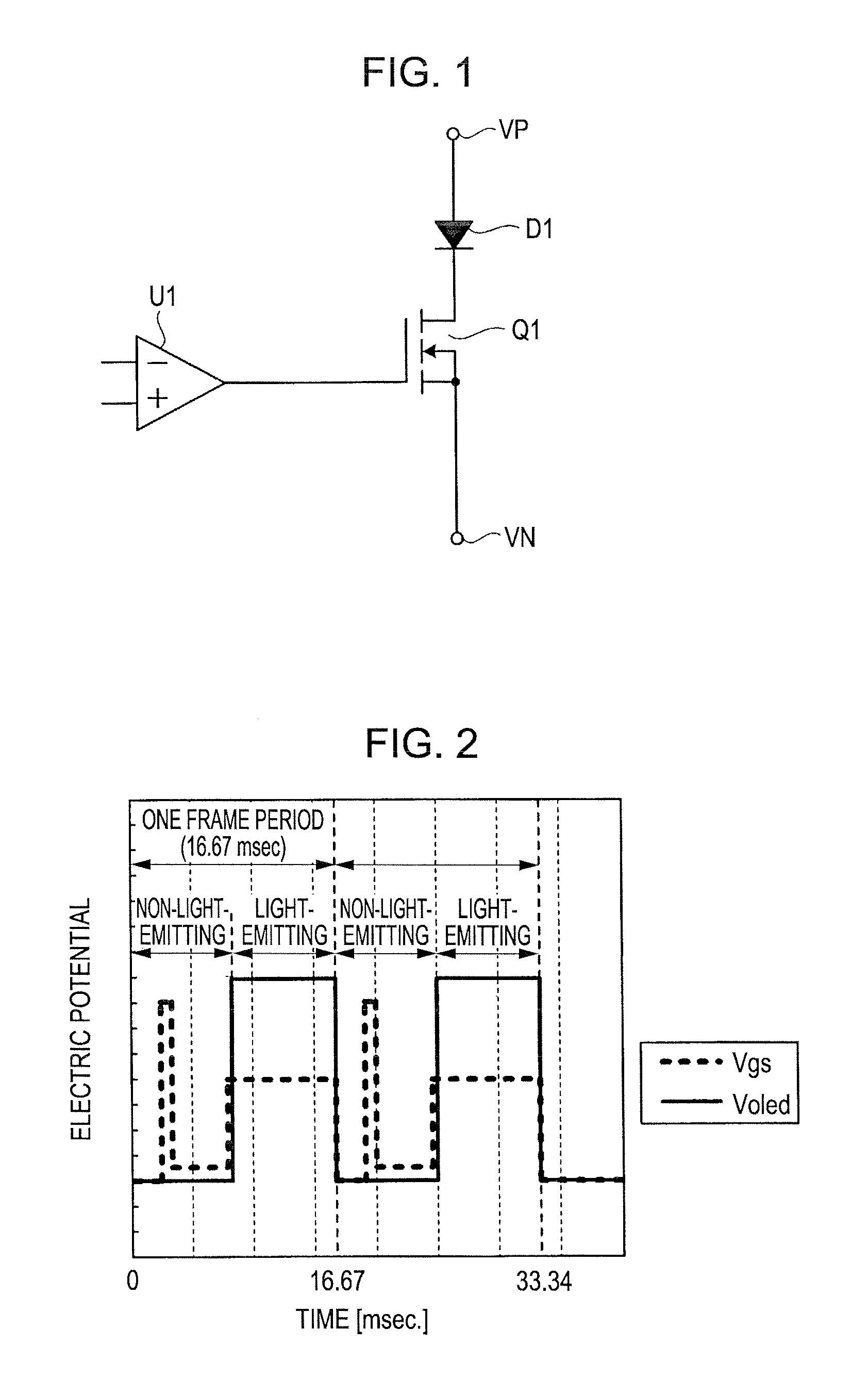
[0041]FIG. 1 is a diagram illustrating an example structure of a pixel circuit corresponding to one pixel of an image display apparatus according to the present embodiment. The pixel circuit shown in FIG. 1 is illustrated in a simple manner.
[0042] The pixel circuit shown in FIG. 1 includes a light emitting element D1, a driver Q1 connected in series to the light emitting element D1, and a controller U1 controlling the driver Q1. The light emitting element D1 is, for example, an organic light emitting element. The light emitting element D1 has an anode connected to a terminal on the high voltage side (hereinafter referred to as a “VP terminal”), and a cathode connected to a drain terminal of the driver Q1 formed of, for example, an aSi-TFT. A source terminal of the driver Q1 is connected to a terminal on the low appli...
example 1
[0070]FIG. 7 is a diagram illustrating the relationship between a lighting time of the driver Q1 in the pixel circuit shown in FIG. 1 and the Vth shift ΔV when no reverse bias voltage was applied to the driver Q1, and FIGS. 8 and 9 are diagrams illustrating the relationship between a lighting time of the driver Q1 in the pixel circuit shown in FIG. 1 and the Vth shift when a reverse bias voltage was applied to the driver Q1. The lighting time means the time during which the driver Q1 is driven so as to have the light emitting element emit light. FIGS. 8 and 9 show the operation with repetitions of a lighting time of 10 minutes and a non-lighting time of 20 minutes. In particular, FIG. 8 shows the case where the reverse bias voltage was “−1 V”, and FIG. 9 shows the case where the reverse bias voltage was “−5 V”.
[0071] As shown in FIG. 7, in the case where no reverse bias voltage was applied, a Vth shift of about 0.8 V was observed under continuous operation for about 60 hours. As sh...
example 2
[0077]FIGS. 10 and 11 are diagrams illustrating characteristics under similar conditions to those shown in FIGS. 7 and 9, respectively. FIG. 10 shows the case where a driver was continuously used for 16 hours during daytime with repetitions of a lighting time of 3 minutes and a non-lighting time of 17 minutes and was in a non-lighting state for 8 hours during nighttime. FIG. 10 shows the case where the gate, source, and drain voltages of the driver were simply released for the non-lighting time during nighttime. On the other hand, FIG. 11 shows the case where the driver was continuously used for 16 hours during daytime with repetitions of a lighting time of 3 minutes and a non-lighting time of 17 minutes and was in a non-lighting state for 8 hours during nighttime. FIG. 11 shows the case where the drain-source voltage was maintained at the same potential for the non-lighting time during nighttime and a reverse bias voltage of −5 V was applied to the gate-source voltage for the initi...
PUM
 Abstract
Description
Claims
Application Information
 - R&D Engineer
- R&D Manager
- IP Professional
- Industry Leading Data Capabilities
- Powerful AI technology
- Patent DNA Extraction
Browse by: Latest US Patents, China's latest patents, Technical Efficacy Thesaurus, Application Domain, Technology Topic, Popular Technical Reports.
© 2024 PatSnap. All rights reserved.Legal|Privacy policy|Modern Slavery Act Transparency Statement|Sitemap|About US| Contact US: help@patsnap.com


