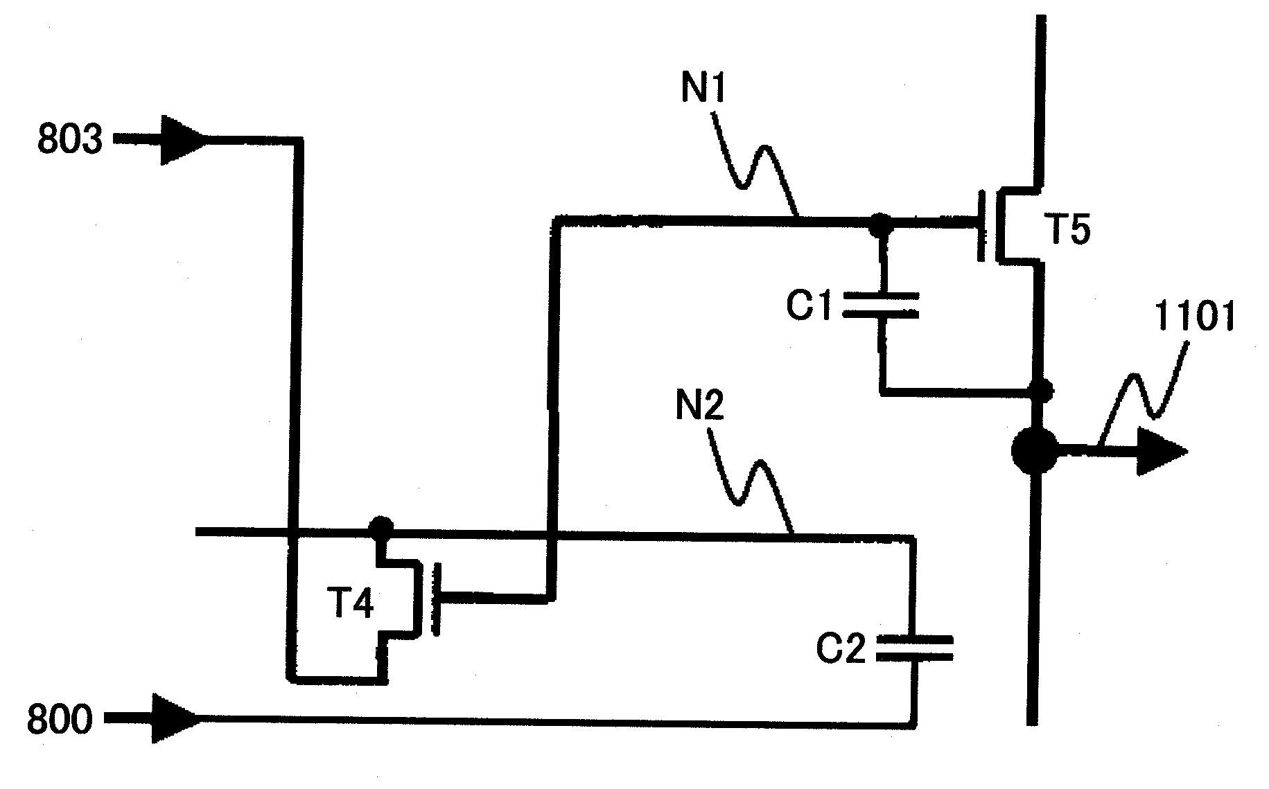
Driver circuit controlling threshold voltage shift of transistor
a transistor and driver circuit technology, applied in the field of display devices, can solve the problems of display errors, node qb floating in the high level, and the ability to supply low-level voltage (vss) to the node qb, and achieve the effect of reducing the shift amount of the threshold voltag
- Summary
- Abstract
- Description
- Claims
- Application Information
AI Technical Summary
Benefits of technology
Problems solved by technology
Method used
Image
Examples
first embodiment
Overall Configuration
[0038]FIG. 11 is a diagram illustrating an internal configuration of a display apparatus according to the first embodiment of the present invention. In the figure, reference numeral 700 designates a display region, 701 and 702 each designate a gate circuit control signal generation block, 703 and 704 each designate a gate circuit (scanning signal line driver circuit) having a shift register circuit corresponding to each line, 705 designates a data driver (video signal line driver circuit) transferring a drain signal, a source signal, and a common signal to each pixel, and 706 designates all data wirings of the drain, source, and common signals which are output from the data driver 705. In the figure, solid arrows represent the flows of gate output signals (scanning signals). In the following description, a display apparatus using a liquid-crystal display will be described as an example of a display apparatus. However, the present invention is not limited to this...
second embodiment
[0081]FIG. 17 is a diagram illustrating a schematic configuration of a shift register circuit in a display apparatus according to a second embodiment of the present invention. The configuration of the shift register circuit according to the second embodiment is the same as that of the first embodiment, except for the configuration of the transistors T3 and T7. Accordingly, in the following description, the configuration of the transistors T3 and T7 will be described in detail.
[0082]As is clear from FIG. 17, in the shift register circuit according to the second embodiment, the transistor T3 has a configuration in which the gate and drain terminals are connected to the wiring 803 to which the second clock signal is applied, and the source terminal is connected to the second potential node N2. Moreover, the transistor T7 has a configuration in which the gate and drain terminals are connected to the wiring 806 to which the start pulse signal is applied, and the source terminal is connec...
PUM
 Abstract
Description
Claims
Application Information
 - R&D Engineer
- R&D Manager
- IP Professional
- Industry Leading Data Capabilities
- Powerful AI technology
- Patent DNA Extraction
Browse by: Latest US Patents, China's latest patents, Technical Efficacy Thesaurus, Application Domain, Technology Topic, Popular Technical Reports.
© 2024 PatSnap. All rights reserved.Legal|Privacy policy|Modern Slavery Act Transparency Statement|Sitemap|About US| Contact US: help@patsnap.com


