Active matrix substrate

a technology of active matrix and substrate, which is applied in the direction of basic electric elements, electrical apparatus, semiconductor devices, etc., can solve the problems of conventionally difficult to keep the sheet resistance of the gate metal layer low, and the sheet resistance of the gate metal layer cannot be reduced to a desired value, so as to improve the adhesion to the surface of the substrate, increase the sheet resistance, and reduce the effect of gate metal layer sheet resistan

Active Publication Date: 2019-09-26
SHARP KK
View PDF7 Cites 0 Cited by
  • Summary
  • Abstract
  • Description
  • Claims
  • Application Information

AI Technical Summary

Benefits of technology

[0091]With the active matrix substrate 1000 of the present embodiment, since the copper alloy layer g1 is provided on the substrate side of the copper layer g2 of the gate metal layer, it is possible to improve the adhesion to the surface of the substrate 1.
[0092]As described above, with a conventional gate metal layer having a Cu / Ti layered metal structure, Ti may possibly diffuse into the Cu layer due to a thermal influence from the TFT process, thereby increasing the sheet resistance. In contrast, in the present embodiment, it is possible to maintain the low sheet resistance of the gate metal layer even after the TFT process is performed. This is because the content of a metal element (e.g., Al) other than Cu of the lower layer of the gate metal layer is suppressed (the total content of additive metal elements is 5% when Cu content is 95%, for example), and therefore even if the metal element diffuses into the copper layer g2, it is possible to suppress the increase in the resistance of the copper layer g2 due to the diffusion. Therefore, it is possible to realize a gate metal layer that has a low sheet resistance and that has a good adhesion.
[0093]The Cu content of the copper alloy layer g1 may be 80 at % or more, for example. Then, since the total content of the additive metal element such as Al is suppressed to be 20 at % or less, it is possible to more effectively suppress the increase in the resistance of the copper layer g2 due to the diffusion of the additive metal element.
[0094]The thickness of the copper alloy layer g1 is preferably 30 nm or more, for example. Then, it is possible to further increase the adhesion to the surface of the substrate 1 (or the base surface). On the other hand, the thickness of the copper alloy layer g1 may be 100 nm or less, for example. Then, it is possible to suppress the increase in the thickness of the gate metal layer as a whole. The thickness of the copper alloy layer g1 may be smaller than the thickness of the copper layer g2. By increasing the thickness of the copper layer g2 having a low electric resistance, it is possible to more effectively lower the sheet resistance of the gate metal layer.
[0095]The present embodiment also provides the following advantage. When forming a conventional gate metal layer having a Cu / Ti layered metal structure, the gate metal layer is patterned by using a hydrogen peroxide-based etchant that contains ammonium fluoride and / or acidic ammonium fluoride, for example. Then, the Cu layer and the Ti layer are both etched. However, when the gate metal layer is formed directly on the glass substrate surface, a surface portion of the glass substrate, which is the base, may also be etched along the gate pattern, thereby lowering the strength of the glass substrate. In contrast, in the present embodiment, the gate metal layer can be patterned by using a hydrogen peroxide-based etchant that does not contain ammonium fluoride or acidic ammonium fluoride. This etchant etches both the copper layer g2 and the copper alloy layer g1, but it does not substantially etch the glass substrate. Therefore, it is possible to suppress the overetch of the glass substrate, and it is therefore possible to ensure strength of the glass substrate.
[0096]Using a hydrogen peroxide-based etchant that does not contain ammonium fluoride or acidic ammonium fluoride also provides an advantage that it is possible to reduce the shift amount of the side surface of the gate metal layer, as compared with a case where a hydrogen peroxide-based etchant that contains ammonium fluoride and / or acidic ammonium fluoride is used.

Problems solved by technology

However, a study by the present inventors revealed that there are cases where the sheet resistance of the gate metal layer cannot be reduced to a desired value even when using a Cu layer.
For example, when a gate metal layer having a Cu / Ti layered metal structure is used in an active matrix substrate, the following problem may occur.
Thus, it is conventionally difficult to keep the sheet resistance of the gate metal layer low.

Method used


Image

  • Active matrix substrate
  • Active matrix substrate
  • Active matrix substrate

Examples


first embodiment

[0064]The present inventors made an in-depth study on realizing a wiring structure with which it is possible to achieve both a low sheet resistance and a high adhesion. As a result, the present inventors found that it is possible to improve the adhesion to the substrate surface while maintaining a low sheet resistance by providing a Cu alloy layer having a predetermined composition on the substrate side of the Cu layer. In the present specification, such a structure is referred to as a “Cu / Cu alloy layered metal structure”.

[0065]An active matrix substrate according to one embodiment of the present invention will now be described with reference to the drawings.

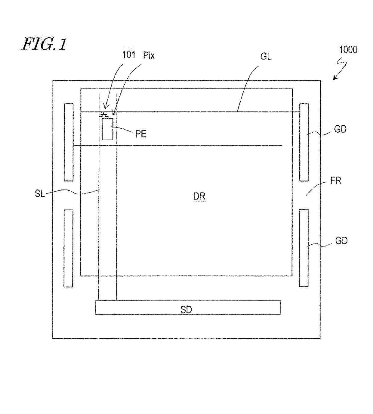
[0066]FIG. 1 is a schematic view showing an example of the planar structure of an active matrix substrate 1000 of the present embodiment.

[0067]The active matrix substrate 1000 has a display region DR, and a region (the non-display region or bezel region) FR other than the display region DR. The display region DR includes pixel ...

second embodiment

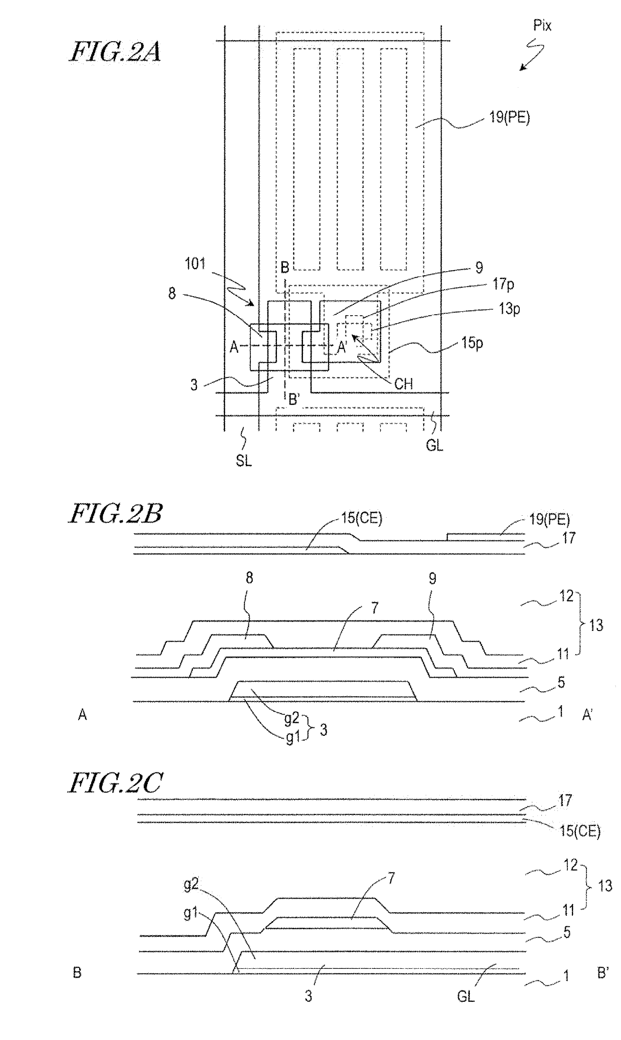
[0136]FIGS. 9A and 9B are cross-sectional views each illustrating an active matrix substrate of the second embodiment.

[0137]With the active matrix substrate of the present embodiment, the gate insulating layer 5 includes the first oxygen-containing silicon layer a1 in direct contact with the oxide semiconductor layer 7, the second oxygen-containing silicon layer a2 in direct contact with the upper surface of the copper layer g2, and the silicon nitride layer n located between the first oxygen-containing silicon layer a1 and the second oxygen-containing silicon layer a2. The gate insulating layer 5 may further include a silicon oxynitride layer (intermediate layer) b between the silicon nitride layer n and the first oxygen-containing silicon layer a1, as illustrated in FIG. 9B. The specific materials and thicknesses of the layers are similar to those described above with reference to FIGS. 8A and 8B, and will not be further described below.

[0138]In the present embodiment, it is only ...

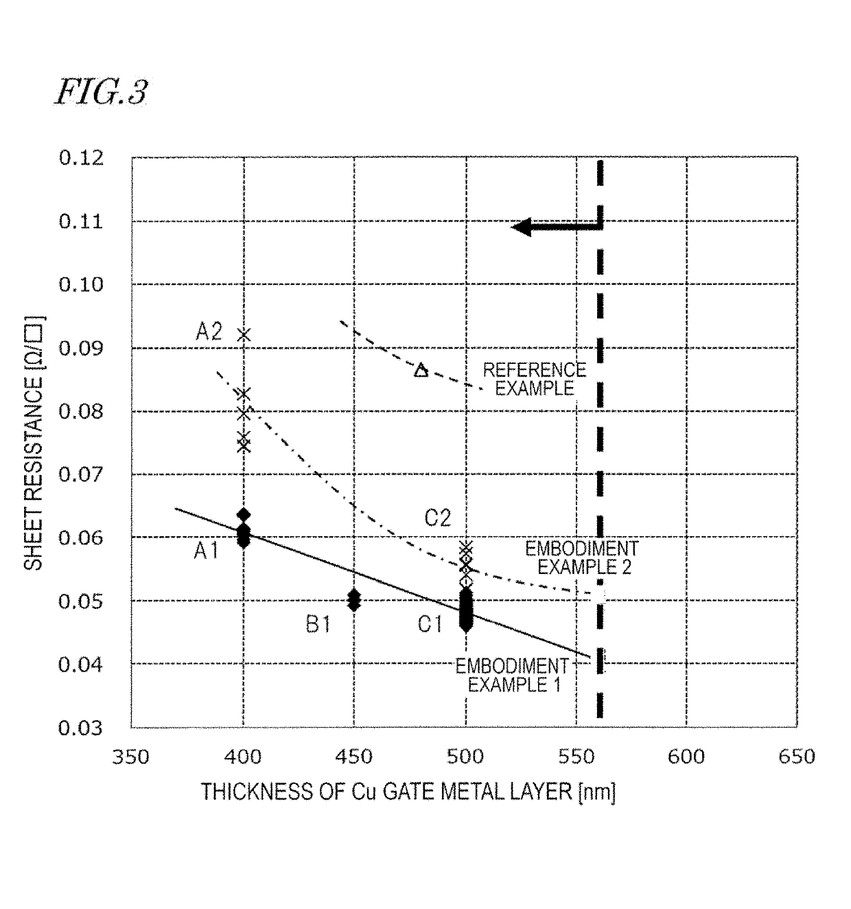
embodiment example and reference example

[0140]

[0141]Active matrix substrates of Embodiment Examples 1 and 2 and Reference Example were produced and compared against each other in terms of the sheet resistance of the gate metal layer.

Method for Manufacturing Active Matrix Substrate of Embodiment Example 1

[0142]First, a gate metal layer having a Cu / Cu alloy layered metal structure was formed on a glass substrate (thickness: 0.7 mm).

[0143]Next, a gate insulating layer including the second oxygen-containing silicon layer a2, the silicon nitride layer n and the first oxygen-containing silicon layer a1 was formed so as to cover the gate metal layer. In Embodiment Example 1, a silicon oxynitride layer (thickness: 100 nm) as the second oxygen-containing silicon layer a2, the silicon nitride layer n (thickness: 300 nm), and a silicon oxide layer (thickness: 50 nm) as the first oxygen-containing silicon layer a1 were formed in this order on the gate metal layer. A plasma CVD method was used for the formation of these films. When fo...


PUM


Abstract

An active matrix substrate includes a source metal layer including a plurality of source bus lines and a gate metal layer including a plurality of gate bus lines, and a thin film transistor arranged in each pixel region, wherein: the thin film transistor includes a gate electrode, an oxide semiconductor layer arranged on the gate electrode with a gate insulating layer interposed therebetween, and a source electrode and a drain electrode, wherein the gate electrode is formed in the gate metal layer and is electrically connected to a corresponding one of the plurality of gate bus lines, the gate metal layer has a layered structure including a copper alloy layer and a copper layer arranged on the copper alloy layer, wherein the copper alloy layer is of a copper alloy including Cu and at least one additive metal element, wherein the additive metal element includes Al, and an Al content of the copper alloy is 2 at % or more and 8 at % or less.

Description

BACKGROUND1. Technical Field[0001]The present invention relates to an active matrix substrate formed by using an oxide semiconductor.2. Description of the Related Art[0002]An active matrix substrate used in a liquid crystal display device, or the like, includes a switching element such as a thin film transistor (hereinafter “TFT”) for each pixel. Conventionally, as such TFTs (hereinafter, “pixel TFTs”), TFTs using an amorphous silicon film as the active layer (hereinafter, “amorphous silicon TFTs”) and TFTs using a polycrystalline silicon film as the active layer (hereinafter, “polycrystalline silicon TFTs”) have been widely used.[0003]On the other hand, techniques are known in the art for monolithically (integrally) providing peripheral circuits such as driving circuits on the substrate. By monolithically forming driving circuits, it is possible to reduce the width of the non-display region and to reduce the cost by simplifying the mounting step. In the present specification, TFTs ...

Claims


Application Information

Patent Timeline
Patent Type & Authority Applications(United States)
IPC IPC(8): H01L27/12H01L29/49H01L29/51
CPCH01L29/4958H01L29/4908H01L29/518H01L27/124H01L27/127H01L27/1225H01L27/1218H01L29/7869
Inventor UEDA, TERUYUKIHARA, YOSHIHITODAITOH, TOHRUIMAI, HAJIMEKITAGAWA, HIDEKIMAEDA, MASAKIKAWASAKI, TATSUYAHIRATA, YOSHIHARUKIKUCHI, TETSUOITOH, TOSHIKATSU
Owner SHARP KK
Why Eureka
Try Eureka