Method for manufacturing printed circuit board
- Summary
- Abstract
- Description
- Claims
- Application Information
AI Technical Summary
Benefits of technology
Problems solved by technology
Method used
Image

Examples
Embodiment Construction
[0031]Embodiments of the method for manufacturing printed circuit board according to the invention will be described below in more detail with reference to the accompanying drawings. In the description with reference to the accompanying drawings, those components are rendered the same reference number that are the same or are in correspondence regardless of the figure number, and redundant explanations are omitted.
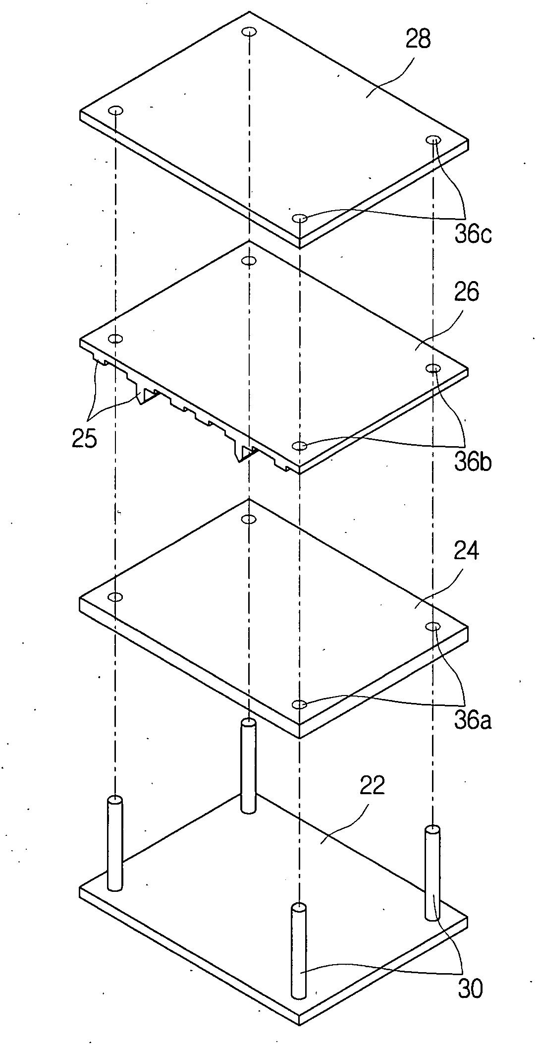
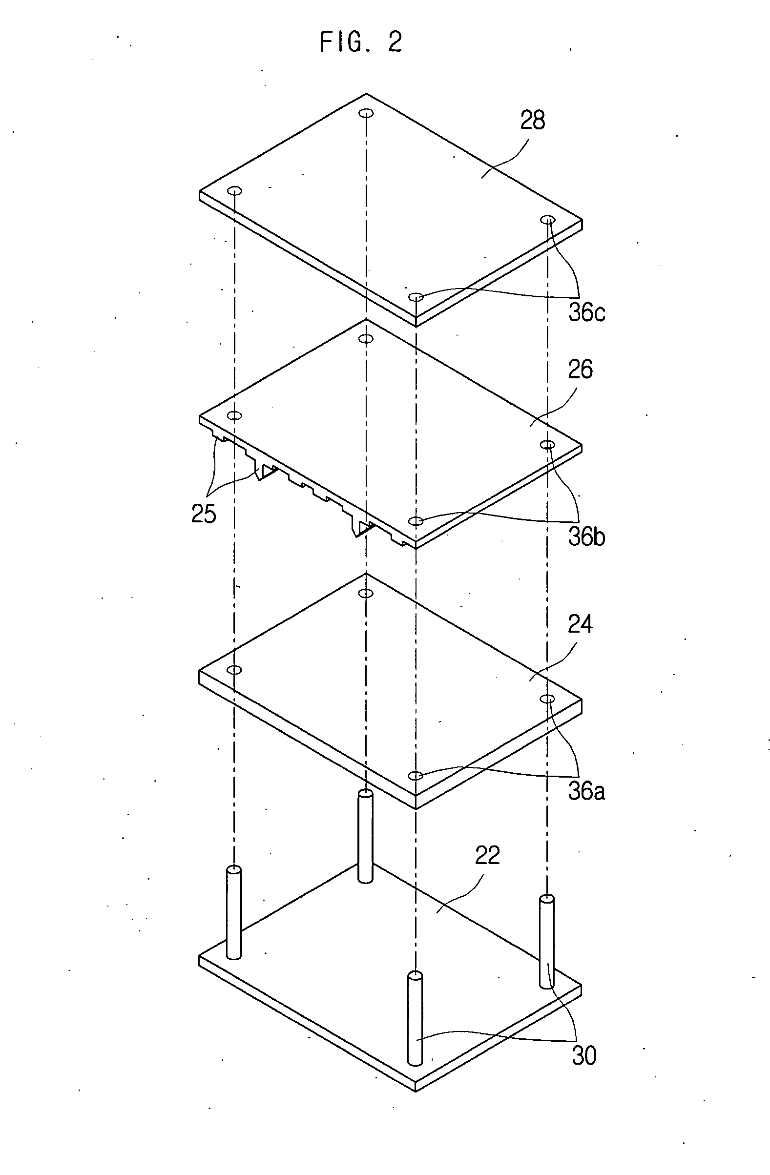
[0032]FIG. 2 is a perspective view showing a method for aligning according to an embodiment of the present invention. FIG. 3 is a side view showing a method for aligning according to an embodiment of the present invention. Referring to FIGS. 2 and 3, a support plate 22, an insulation substrate 24, an imprinting mold 26, a pressing plate 28, guide pins 30, a raised pattern 25 and align holes 36a, 36b, 36c are illustrated.
[0033]In this embodiment, an insulation substrate 24 having first align holes 36a perforated is stacked onto a support plate 22 having guide pins 30 joined...
PUM
| Property | Measurement | Unit |
|---|---|---|
| Electrical conductor | aaaaa | aaaaa |
Abstract
Description
Claims
Application Information
 - Generate Ideas
- Intellectual Property
- Life Sciences
- Materials
- Tech Scout
- Unparalleled Data Quality
- Higher Quality Content
- 60% Fewer Hallucinations
Browse by: Latest US Patents, China's latest patents, Technical Efficacy Thesaurus, Application Domain, Technology Topic, Popular Technical Reports.
© 2025 PatSnap. All rights reserved.Legal|Privacy policy|Modern Slavery Act Transparency Statement|Sitemap|About US| Contact US: help@patsnap.com