Substrate strip

Active Publication Date: 2014-08-28
SAMSUNG ELECTRO MECHANICS CO LTD
View PDF2 Cites 0 Cited by
  • Summary
  • Abstract
  • Description
  • Claims
  • Application Information

AI Technical Summary

Benefits of technology

[0014]An object of the present invention is to provide a substrate strip capable of preventi

Problems solved by technology

However, the chip itself may not receive electricity supplied from the outside to transmit and receive an electric signal.
In addition, since the chip includes fine circuits, it is easily damaged due to external impact.
Close adhesion force between the substrate strip and the molding clamp is decreased due to the deformation of the substrate strip an

Method used


Image

  • Substrate strip
  • Substrate strip
  • Substrate strip

Examples


Embodiment Construction

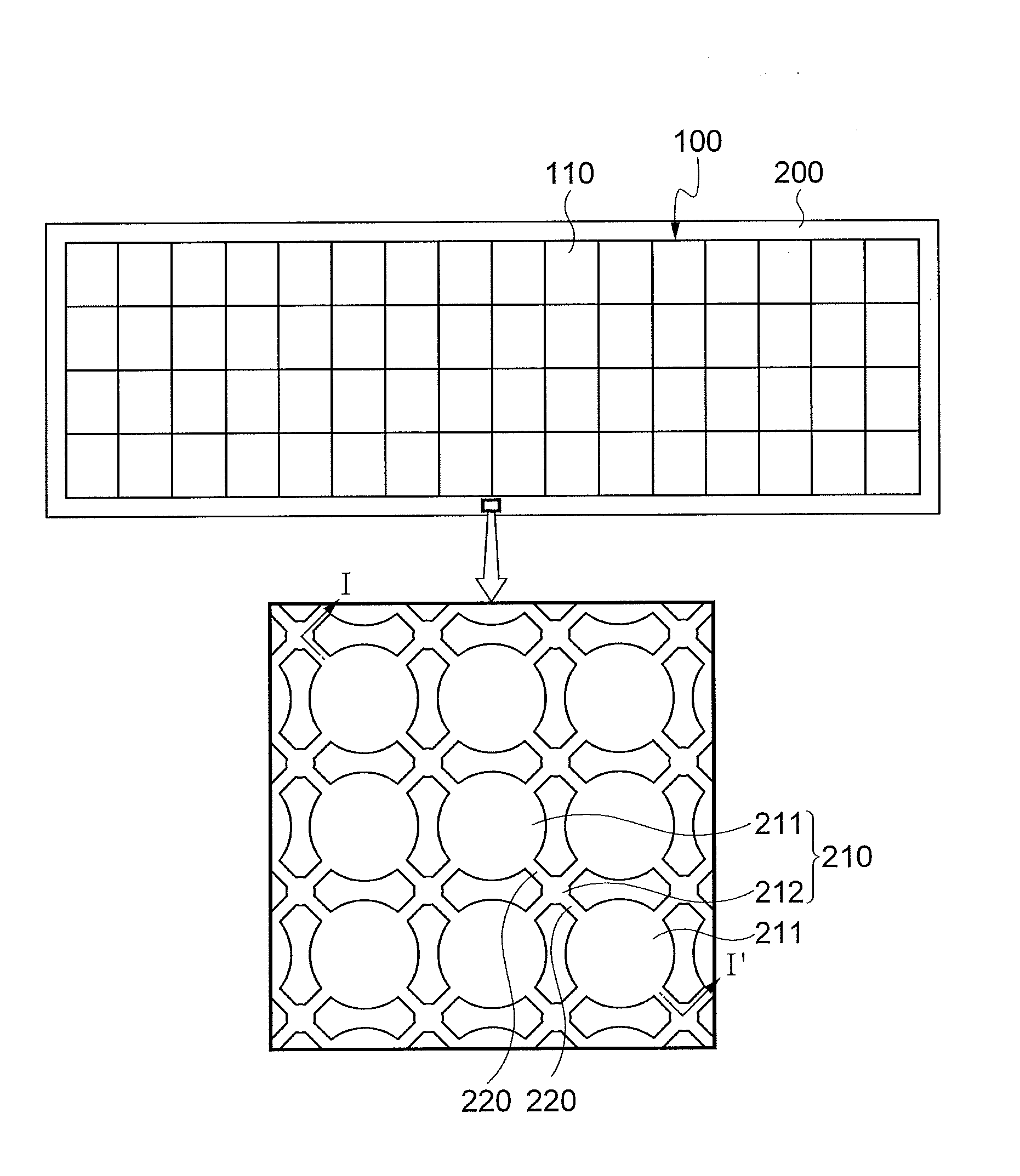
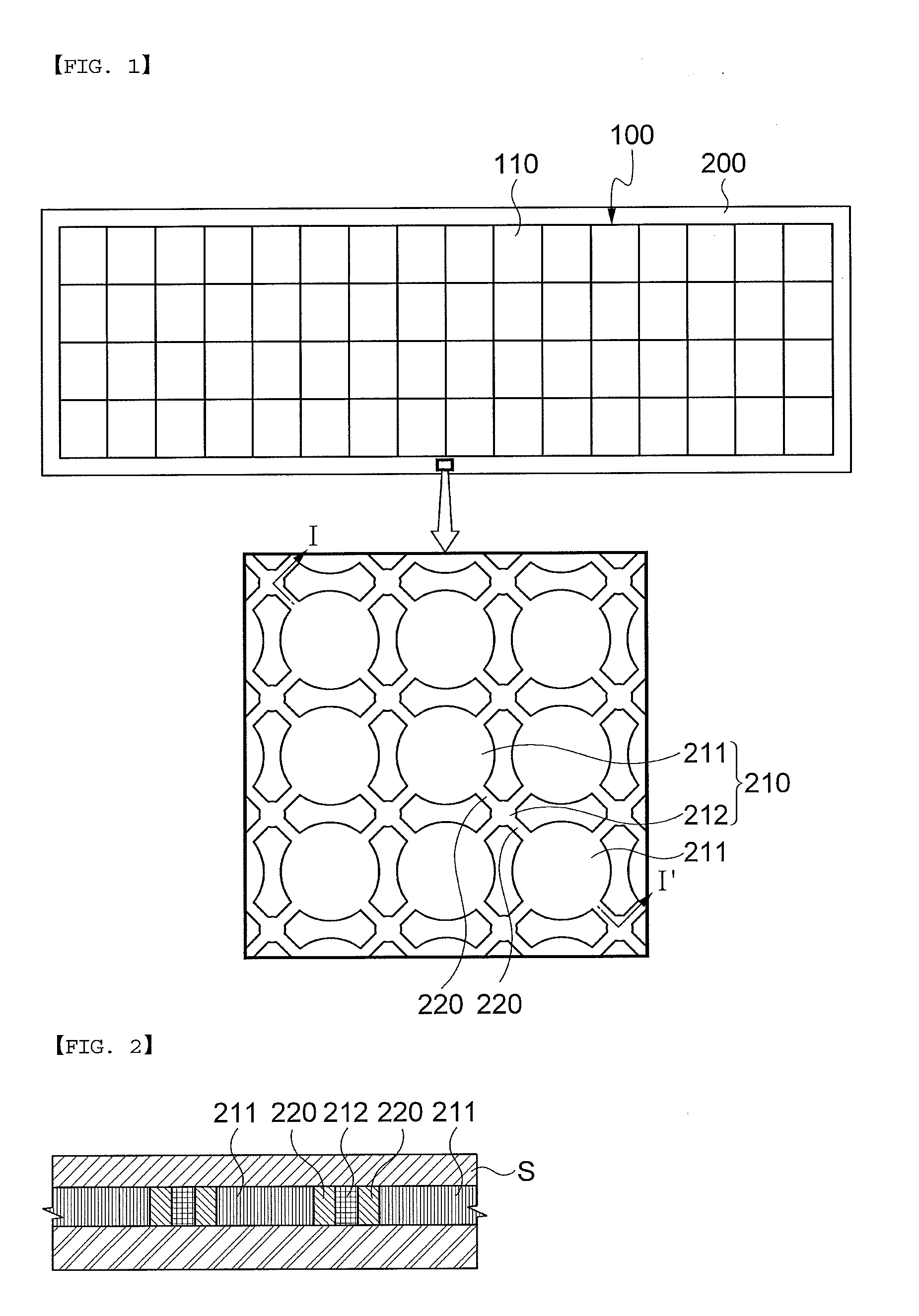
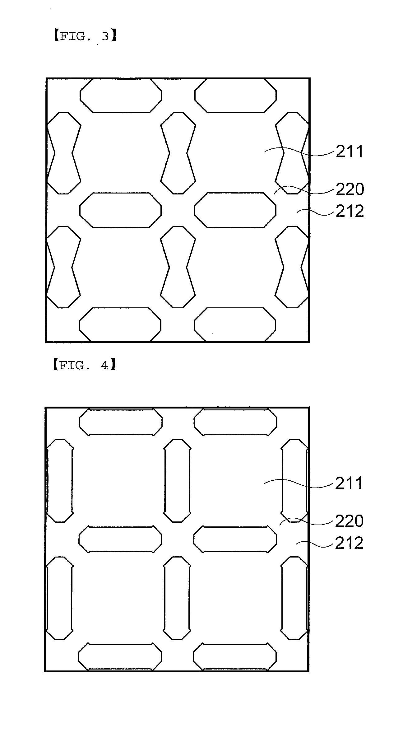
[0034]Hereinafter, exemplary embodiments of the present invention will be described with reference to the accompanying drawings. However, the exemplary embodiments are described by way of examples only and the present invention is not limited thereto.

[0035]In describing the present invention, when a detailed description of well-known technology relating to the present invention may unnecessarily make unclear the spirit of the present invention, a detailed description thereof will be omitted. Further, the following terminologies are defined in consideration of the functions in the present invention and may be construed in different ways by the intention of users and operators. Therefore, the definitions thereof should be construed based on the contents throughout the specification.

[0036]As a result, the spirit of the present invention is determined by the claims and the following exemplary embodiments may be provided to efficiently describe the spirit of the present invention to thos...


PUM


Abstract

Disclosed herein is a substrate strip including: a substrate region having a plurality of substrate units formed therein; a dummy region enclosing the substrate region; a plurality of metal patterns formed at a predetermined size in the dummy region; and rib patterns formed between the metal patterns.

Description

CROSS REFERENCE(S) TO RELATED APPLICATIONS[0001]This application claims the benefit under 35 U.S.C. Section 119 of Korean Patent Application Serial No. 10-2013-0019129, entitled “Substrate Strip” filed on Feb. 22, 2013, which is hereby incorporated by reference in its entirety into this application.BACKGROUND OF THE INVENTION[0002]1. Technical Field[0003]The present invention relates to a substrate strip, and more particularly, to a substrate strip in which units having semiconductor chips mounted thereon are disposed in at least one row.[0004]2. Description of the Related Art[0005]Generally, several tens to several hundreds of chips may be formed per one wafer. However, the chip itself may not receive electricity supplied from the outside to transmit and receive an electric signal. In addition, since the chip includes fine circuits, it is easily damaged due to external impact.[0006]Therefore, a packaging technology of performing electrical connection to the chips and protecting the...

Claims


Application Information

Patent Timeline
IPC IPC(8): H05K7/02
CPCH05K7/02H01L21/561H01L23/3107H01L23/49838H01L24/97H01L21/02H01L23/12
Inventor KIM, JOONG SUNPARK, SANG GABYOUM, KWANG SEOP
Owner SAMSUNG ELECTRO MECHANICS CO LTD
Why Eureka
Try Eureka