

Wafer and semiconductor device testing method
- Summary
- Abstract
- Description
- Claims
- Application Information
AI Technical Summary
Benefits of technology
Problems solved by technology
Method used
Image

Examples
Embodiment Construction
[0042] The present invention will be described in detail below by the embodiment shown in the drawings.
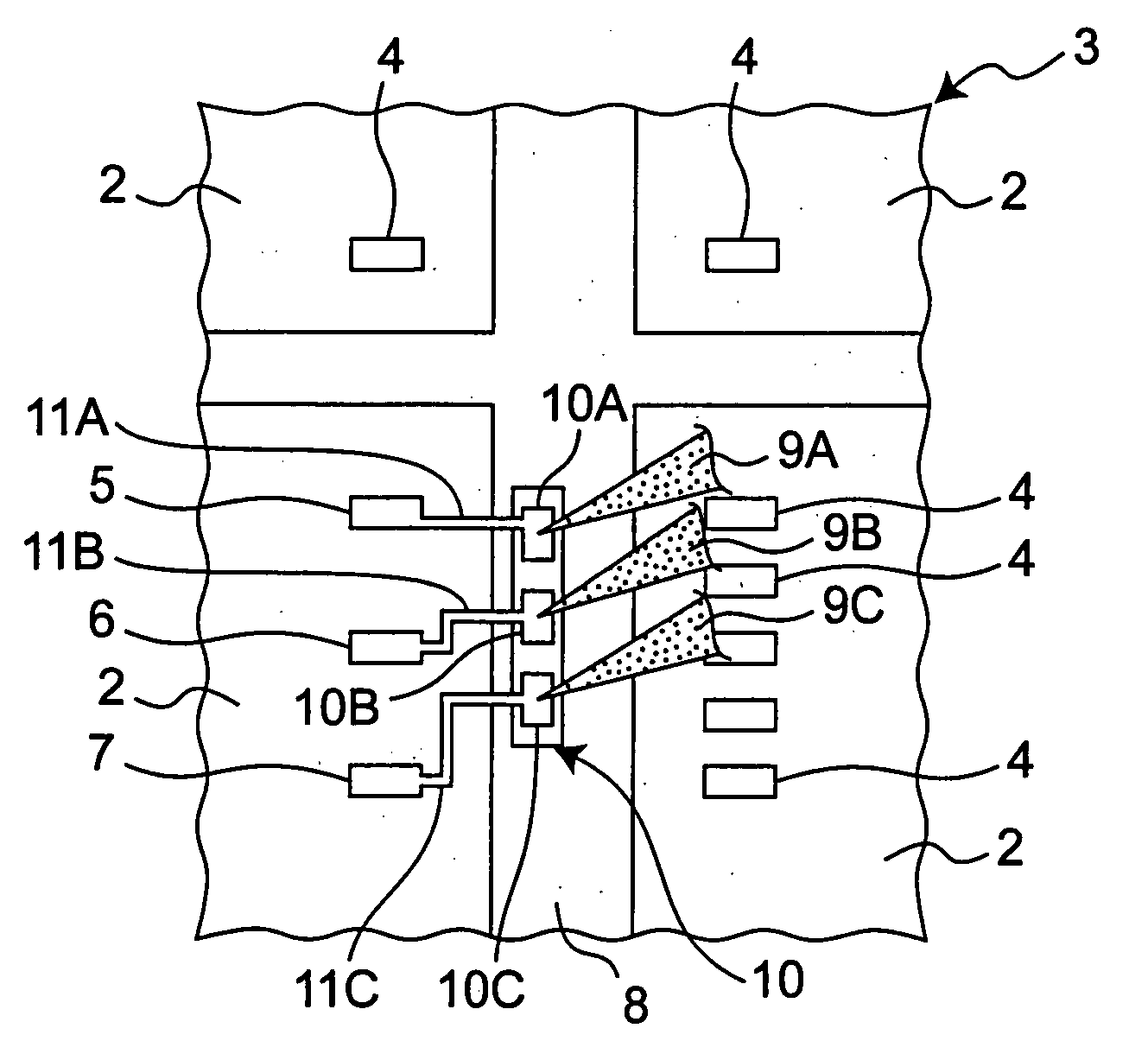
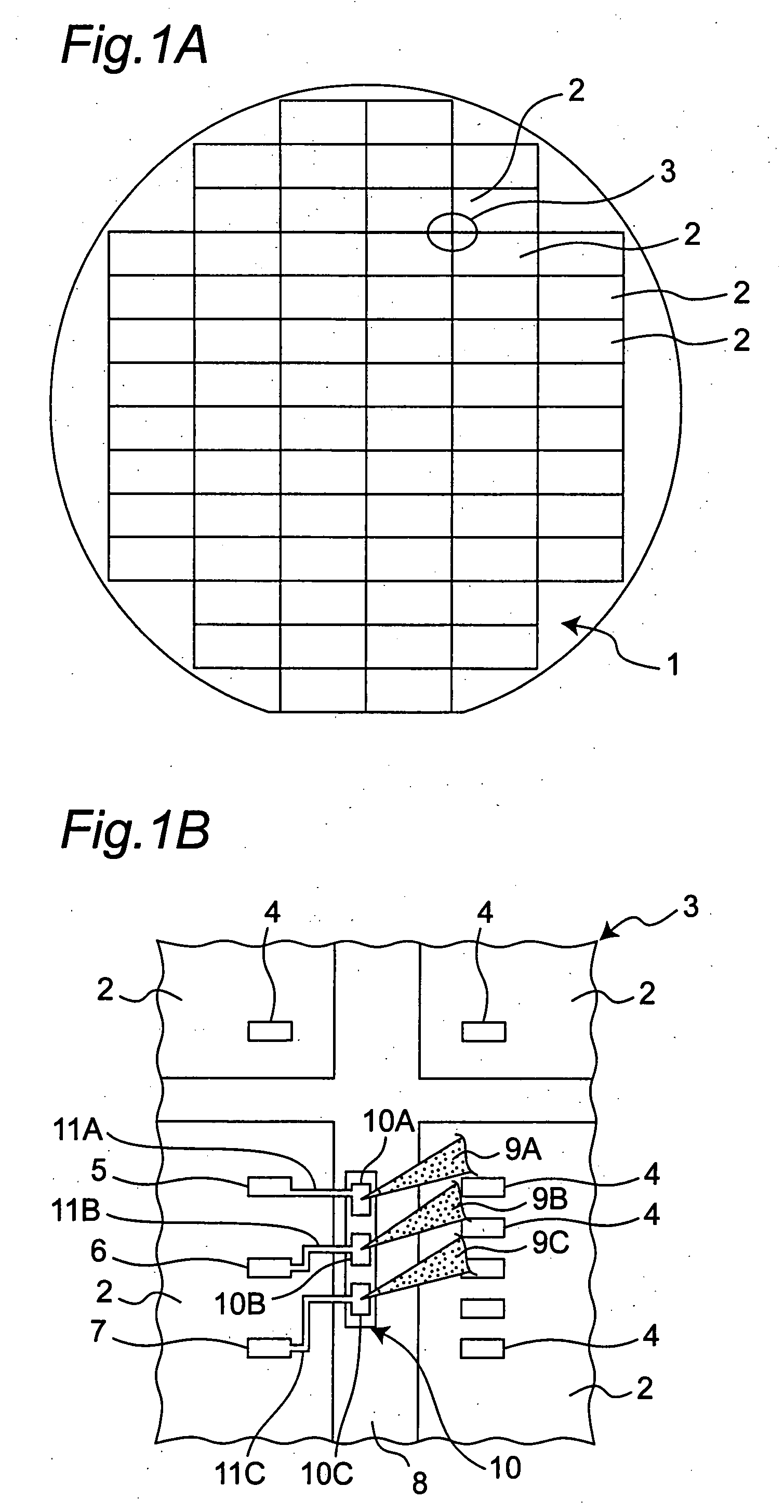
[0043]FIG. 1A shows the schematic construction of a wafer 1 according to one embodiment of the present invention. The wafer 1 has undergone a wafer process, and the wafer surface is segmented into a plurality of rectangular regions (referred to as “chip regions”) 2 as in a general wafer. A semiconductor device (not shown) is fabricated in each of the chip regions 2.
[0044]FIG. 1B shows a part of FIG. 1A, i.e., a portion 3 where corner portions of four chip regions 2 gather. As shown in FIG. 1B, the chip regions 2 are partitioned by a scribe line (also referred to as a dicing line) 8 that has a certain width between the chip regions. It is noted that the wafer 1 is segmented into chips along the scribe line 8 after finishing a wafer test described later. A plurality of pads 4 for inputting and outputting signals between the elements in the chip regions and the outside are arranged ...
PUM
 Abstract
Description
Claims
Application Information