Prober and probe contact method

a probe and contact method technology, applied in the direction of individual semiconductor device testing, semiconductor/solid-state device testing/measurement, instruments, etc., can solve the problems of troublesome inspection, difference in the contact position between the probe and the electrode, etc., to reduce the error in the contact position, accurately predict the change in the temperature of the wafer, and accurately maintain the

Inactive Publication Date: 2008-01-24
TOKYO SEIMITSU
View PDF1 Cites 17 Cited by
  • Summary
  • Abstract
  • Description
  • Claims
  • Application Information

AI Technical Summary

Benefits of technology

[0017]For a probing test at a high or low temperature, a temperature range is specified. Because of this, for example, the set temperature T1 of the wafer chuck 18 is adjusted so that it is at a middle temperature of the temperature range and a probing test is started when the temperature of the wafer W reaches the lower limit (T1-ΔT) of the temperature range or becomes higher. In addition, if the set temperature T1 of the wafer chuck 18 is adjusted to a temperature near the upper limit of the temperature range, it is possible to shorten the time required for the temperature of the wafer W to reach the lower limit of the temperature range.
[0019]In order to prevent such problems from occurring, one measure is to not carry out the wafer alignment operation until the temperature of the wafer W approaches the set temperature. Due to this, the dimensional error resulting from the change in the temperature of the wafer W is small because the change in the temperature between when the wafer alignment operation has been carried out and when the probing test is conducted is small. However, waiting for such a long period of time will lower the throughput of the prober and raise cost.
[0020]The present invention will solve these problems and an object thereof is to reduce the error in the contact position between a probe and an electrode without lowering throughput when a probing test of a wafer is conducted at a high or low temperature.
[0024]According to the present invention, the change in the temperature of the wafer after it is held on the wafer chuck is predicted and the change in the dimension of the wafer in accordance with the change in the temperature of the wafer is predicted and then the amount of movement is corrected, and therefore, it is possible to reduce the error in the contact position between the probe and the electrode.
[0025]A wafer is thin and plate-shaped and its undersurface is comparatively similar, and therefore, if the condition is the same, it changes similarly. If the wafer temperature change after the wafers at various temperatures are held on the wafer chuck and the temperature change data about the change in dimension are measured and stored in advance for each condition, such as the wafer's thickness, diameter, material, etc., it is possible to accurately predict the change in temperature of a wafer. Specifically, how it changes differs depending on the condition, such as wafer's thickness, diameter, material, etc., and therefore, the temperature change data is measured and stored in advance about these conditions and combinations of the initial temperature of a wafer and the set temperature of the wafer chuck. When a silicon wafer of the same specifications is used, since the diameter and the material are the same, it is only necessary to measure and store the temperature change data in advance under the condition of wafer's thickness and to measure the thickness of the wafer and the temperature of the wafer before it is held, and thus the temperature of the wafer chuck is accurately maintained at a set temperature.
[0026]According to the present invention, when a probing test of a wafer is conducted at a high or low temperature, it is possible to reduce an error in the contact position between a probe and an electrode without lowering throughput.

Problems solved by technology

However, even after wafer alignment is carried out, the temperature of the wafer W changes gradually, and therefore, a dimensional error occurs because the temperature of the wafer W when the wafer alignment operation has been carried out is different from that when the probing test is conducted, resulting in a difference in the contact position between the probe and the electrode, and there may be trouble with the inspection.

Method used


Image

  • Prober and probe contact method
  • Prober and probe contact method
  • Prober and probe contact method

Examples


Embodiment Construction

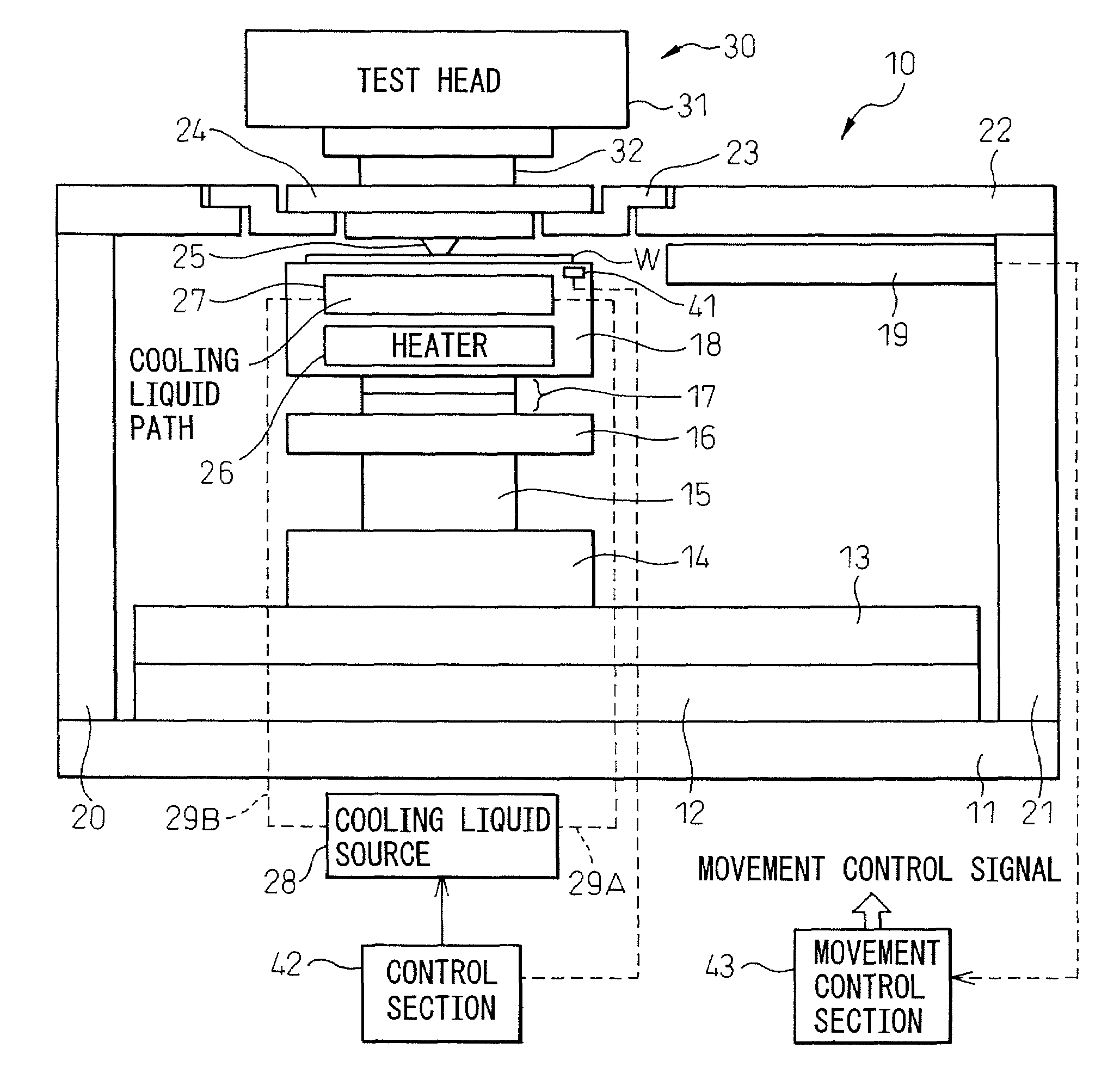
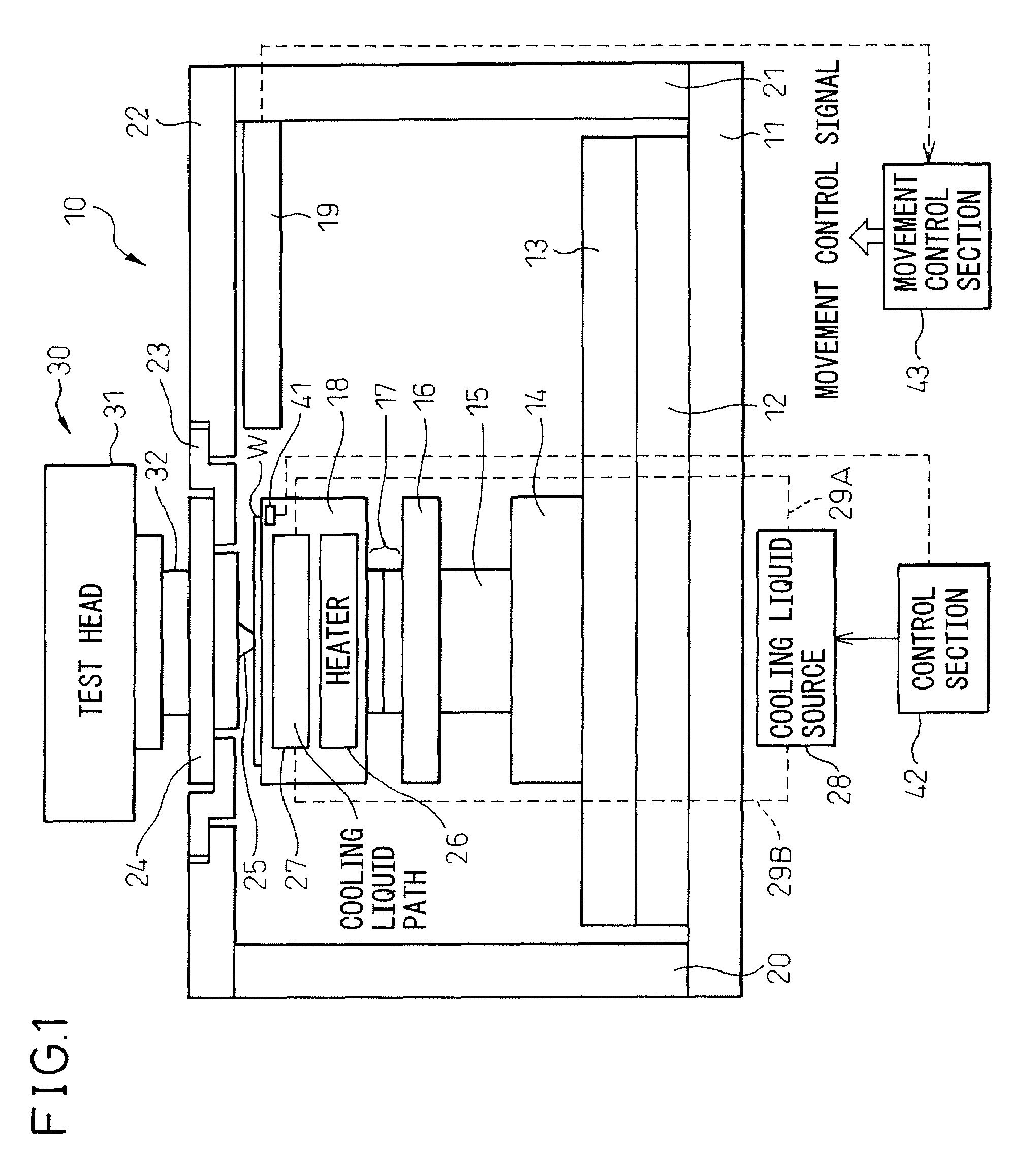
[0033]The prober in an embodiment of the present invention has the same configuration as that in the conventional example shown in FIG. 1 and only the configuration of the movement control section 43 is different. FIG. 4 is a block diagram showing the configuration of the prober movement control section 43 in the embodiment of the present invention.

[0034]The prober movement control section 43 calculates an amount of movement to touch an electrode to a probe based on the result of alignment operation and carries out the conventional process to control the movement / rotation mechanism and at the same time, as shown in FIG. 4, the prober movement control section 43 has a movement amount correction section 44 and a temperature change data storage section 45 and corrects the amount of movement calculated by the conventional method.

[0035]The temperature change data storage section 45 stores temperature change data. The temperature change data includes the wafer temperature changes after th...


PUM


Abstract

A prober and a probe contact method for reducing errors in the contact position between a probe and an electrode without lowering throughput when conducting a probing test of a wafer at a high or low temperature have been disclosed. The prober comprises: a wafer chuck that holds a wafer; a movement mechanism that moves the wafer chuck; a temperature adjustment mechanism that adjusts the temperature of the wafer chuck to maintain the wafer at a predetermined temperature; an alignment means for measuring a positional relationship between the electrode of the device of the wafer and the probe; and a movement control section that calculates the amount of movement to touch the electrode to the probe based on the positional relationship between the electrode and the probe measured by the alignment means and controls the movement mechanism based on the calculated amount of movement, wherein: a wafer temperature sensor that detects the temperature of the wafer before it is held on the wafer chuck is further provided; and the movement control section comprises: a temperature change data storage section that stores in advance the wafer temperature changes after the wafers at various temperatures are held on the wafer chuck and the data about the changes in dimension; and a movement amount correction means for predicting the change in temperature after the wafer is held on the wafer chuck from the temperature of the wafer detected by the wafer temperature sensor and the data stored in the temperature change data storage means and corrects the calculated amount of movement in accordance with the predicted change in temperature when making an inspection while maintaining the temperature of the wafer chuck at a low or high set temperature.

Description

BACKGROUND OF THE INVENTION[0001]The present invention relates to a prober that connects an electrode of a die to a probe to be connected to a terminal of a tester in order to conduct electrical inspection of a plurality of devices (dies) formed on a semiconductor wafer and a probe contact method for touching a probe to an electrode, and more particularly, to a prober that inspects a wafer while maintaining it at a high or low temperature and a probe contact method therefor.[0002]In a semiconductor manufacturing process, a plurality of devices (dies) are formed by subjecting a thin disk-shaped semiconductor wafer to various processes. After the electrical characteristic of each device is inspected and the devices are separated using a dicer, they are fixed on a lead frame, etc., and then assembled. The above-mentioned inspection of the electrical characteristics are conducted by a wafer test system consisting of a prober and a tester. This inspection is referred to as a probing test...

Claims


Application Information

Patent Timeline
Patent Type & Authority Applications(United States)
IPC IPC(8): G01R31/02G01R1/067
CPCG01R31/2865H01L22/00
Inventor CHIBA, KIYOTAKAMASE, FUMIO
Owner TOKYO SEIMITSU
Why Eureka
Try Eureka