Liquid crystal display device, liquid crystal display and method of driving liquid crystal display device

a liquid crystal display and display device technology, applied in the direction of instruments, computing, electric digital data processing, etc., can solve the problems of difficulty in actually achieving parameters and insufficient technique to reduce phenomena, and achieve the effect of reducing alignment disorder and high-quality images

Inactive Publication Date: 2008-01-24
SONY CORP
View PDF2 Cites 72 Cited by
  • Summary
  • Abstract
  • Description
  • Claims
  • Application Information

AI Technical Summary

Benefits of technology

[0010]In view of the foregoing, it is desirable to provide an image display device, an image display and a method of driving an image display device capable of reducing the occurrence of alignment disorder of a liquid crystal irrespective of the details of an image so as to display a high-quality image.
[0011]According to an embodiment of the invention, there is provided a liquid crystal display device including: a liquid crystal display panel including a plurality of pixels for displaying images; and a drive means for driving the liquid crystal display panel while correcting pixel data of each pixel one after another, so that a voltage ratio between a voltage applied to one pixel and a voltage applied to its neighboring pixel is reduced.
[0017]In the liquid crystal display device, the liquid crystal display and the method of driving a liquid crystal display device according to the embodiment of the invention, pixel data of each pixel is corrected one after another so that the voltage ratio between a voltage applied to one pixel and a voltage applied to its neighboring pixel is reduced, and t the liquid crystal panel is driven on the basis of pixel data corrected, so the occurrence of the alignment disorder (disclination) of the liquid crystal due to the voltage ratio between the voltages applied to neighboring pixels can be reduced, and a deterioration in image reproducibility can be prevented. Therefore, irrespective of the details of an image, a high-quality image can be displayed.

Problems solved by technology

However, in D. Cuypers et al, a method of achieving such a parameter is not specifically described, so it is difficult to actually achieve the parameter.
However, the technique is not sufficient to reduce the phenomenon while dealing with ever-changing drive conditions of neighboring pixels.

Method used


Image

  • Liquid crystal display device, liquid crystal display and method of driving liquid crystal display device
  • Liquid crystal display device, liquid crystal display and method of driving liquid crystal display device
  • Liquid crystal display device, liquid crystal display and method of driving liquid crystal display device

Examples


first embodiment

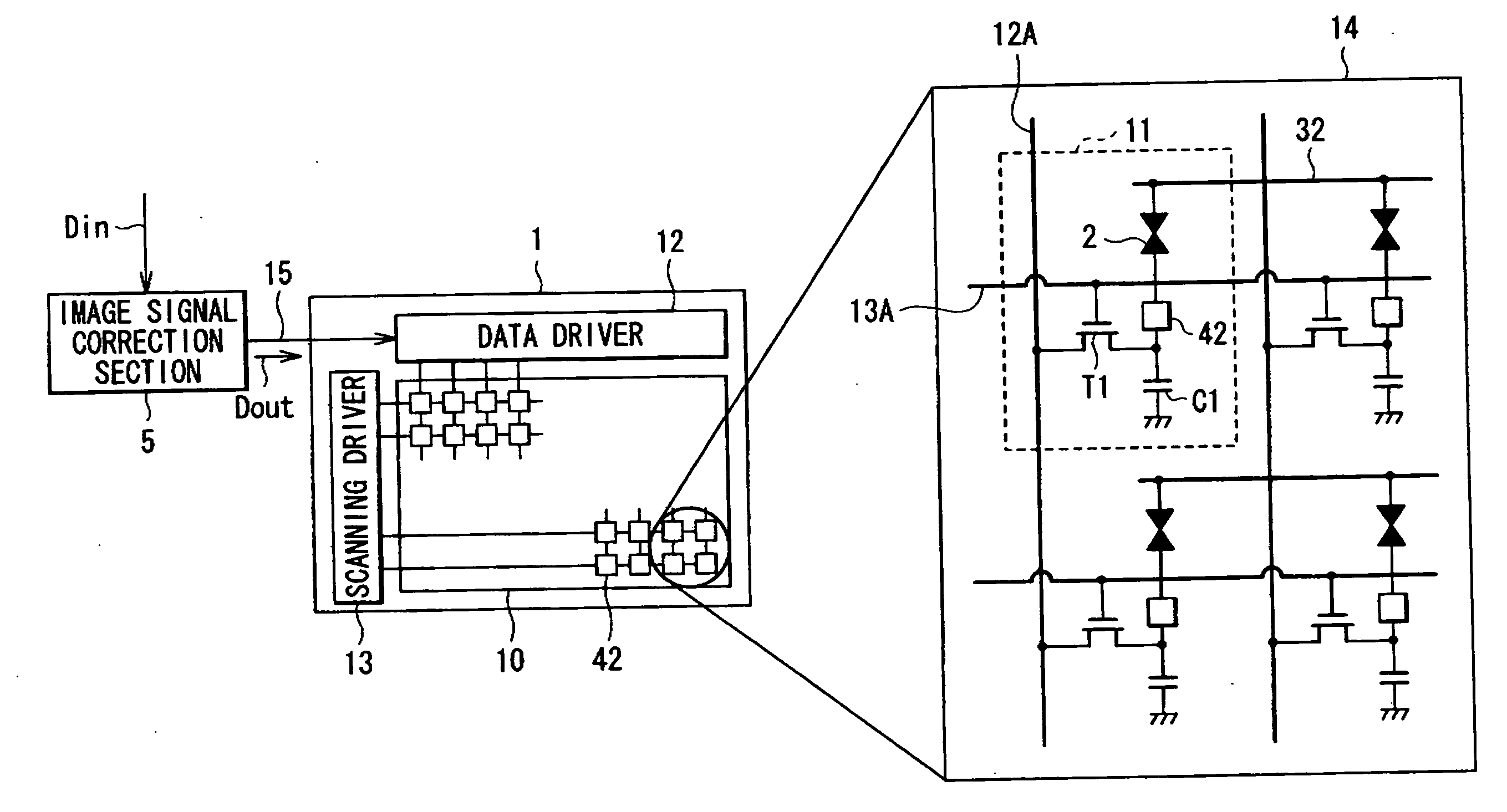
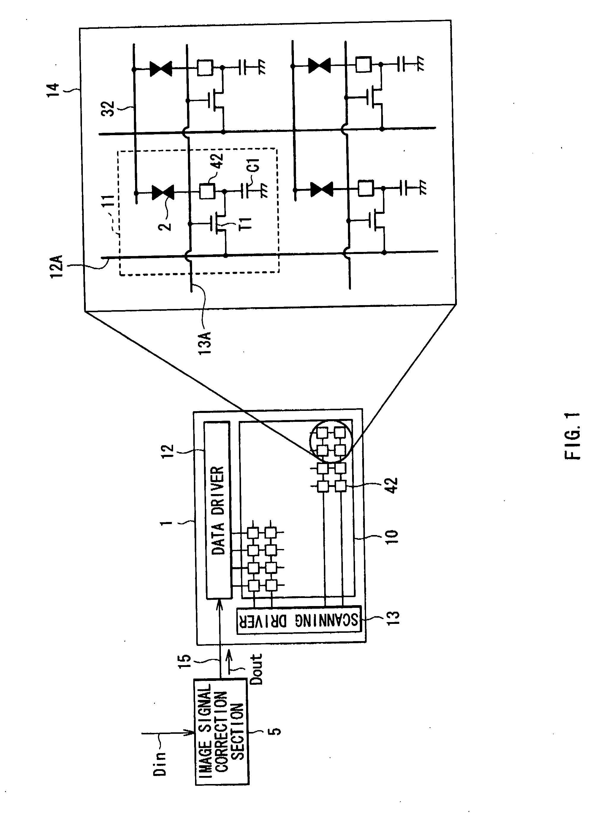
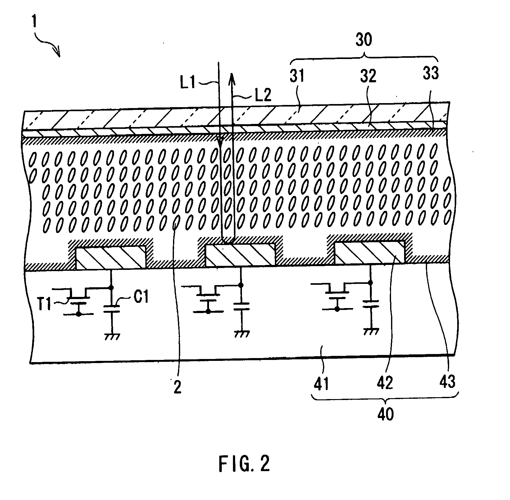
[0039]FIG. 1 shows the configuration of a liquid crystal display device according to a first embodiment of the invention. The liquid crystal display device includes an image signal correction section 5 performing predetermined correction on an input image signal Din from outside and a liquid crystal display section 1 displaying an image on the basis of an image signal (an output image signal Dout) corrected by the image signal correction section 5, and the liquid crystal display device is a reflective type liquid crystal display device as will be described later.

[0040]The liquid crystal display section 1 includes a display region 10 in which a plurality of pixels 11 are arranged in a matrix form, and a data driver 12 and a scanning driver 13 as drivers for image display.

[0041]A pixel drive circuit 14 is formed in each pixel 11, and the above-described data driver 12 and the above-described scanning driver 13 are arranged around the display region 10. The output image signal Dout fro...

second embodiment

[0087]Next, a second embodiment of the invention will be described below. In the first embodiment, a so-called analog system liquid crystal display device in which an applied voltage (a drive voltage) is changed on the basis of pixel data is described. On the other hand, in the embodiment, a so-called digital system liquid crystal display device in which a drive by PWM (Pulse Width Modulation) is performed on the basis of pixel data will be described below.

[0088]FIG. 11 shows a timing chart of a method of driving a typical digital system (in this case, 128 (=2 to the seventh power) gray-level / 7-bit drive system) liquid crystal display device, and (A) through (H) show 1 gray level (=pixel data of “0000001”; a black level), 2 gray levels (=pixel data of “0000010”), 4 gray levels (=pixel data of “0000100”), 8 gray levels (=pixel data of “0001000”), 16 gray levels (=pixel data of “0010000”), 32 gray levels (=pixel data of “0100000”), 64 gray level (=pixel data of “1000000”) and 127 gray...

examples 1-1 , 1-2

Examples 1-1, 1-2

[0099]Test samples of the reflective type liquid crystal display device were formed basically by the same method and the same specifications as those in Comparative Example 1. However, in Examples 1-1 and 1-2, unlike Comparative Example 1, as described in FIGS. 6A and 6B through FIG. 8 or FIG. 9 in the first embodiment, while correction was performed so that the voltage ratio between neighboring pixels was reduced as small as possible, images of pixel patterns shown in FIGS. 15A and 15B were displayed.

[0100]Table 1 shows an example of measurement results of the reflection efficiency E and the contrast C in Comparative Example 1 and Examples 1-1 and 1-2 (in the case where a voltage before correcting one of neighboring pixels was V40). In this case, it was considered that when the reflection efficiency E was 0.70 or more, and the contrast C was 0.60 or more, a displayed image could have sufficient quality for practical use. It was confirmed that while the reflection e...


PUM


Abstract

An image display device capable of displaying a high-quality image by reducing the occurrence of alignment disorder of a liquid crystal irrespective of details of the image is provided. A liquid crystal display device includes: a liquid crystal display panel including a plurality of pixels for displaying images; and a drive means for driving the liquid crystal display panel while correcting pixel data of each pixel one after another, so that a voltage ratio between a voltage applied to one pixel and a voltage applied to its neighboring pixel is reduced.

Description

CROSS REFERENCES TO RELATED APPLICATIONS[0001]The present invention contains subject matter related to Japanese Patent Application JP 2006-195176 filed in the Japanese Patent Office on Jul. 18, 2006, the entire contents of which being incorporated herein by reference.BACKGROUND OF THE INVENTION[0002]1. Field of the Invention[0003]The present invention relates to an active matrix type liquid crystal display device, a liquid crystal display displaying an image through the use of the liquid crystal display device, and a method of driving the liquid crystal display device.[0004]2. Description of the Related Art[0005]In recent years, liquid crystal displays using a liquid crystal as a display device have been widely used. As the liquid crystal displays, for example, there have been commercialized various liquid crystal displays capable of providing a high-resolution image such as a so-called direct-view type liquid crystal display in which a liquid crystal drive circuit is formed on a la...

Claims


Application Information

Patent Timeline
Patent Type & Authority Applications(United States)
IPC IPC(8): G09G5/00G09G3/36
CPCG09G3/2014G09G3/3648G09G2320/0276G09G2320/0209G09G2320/0233G09G2300/0491
Inventor FUJINO, YUSUKE
Owner SONY CORP
Why Eureka
Try Eureka