Pad structure for liquid crystal display and method of manufacturing thereof

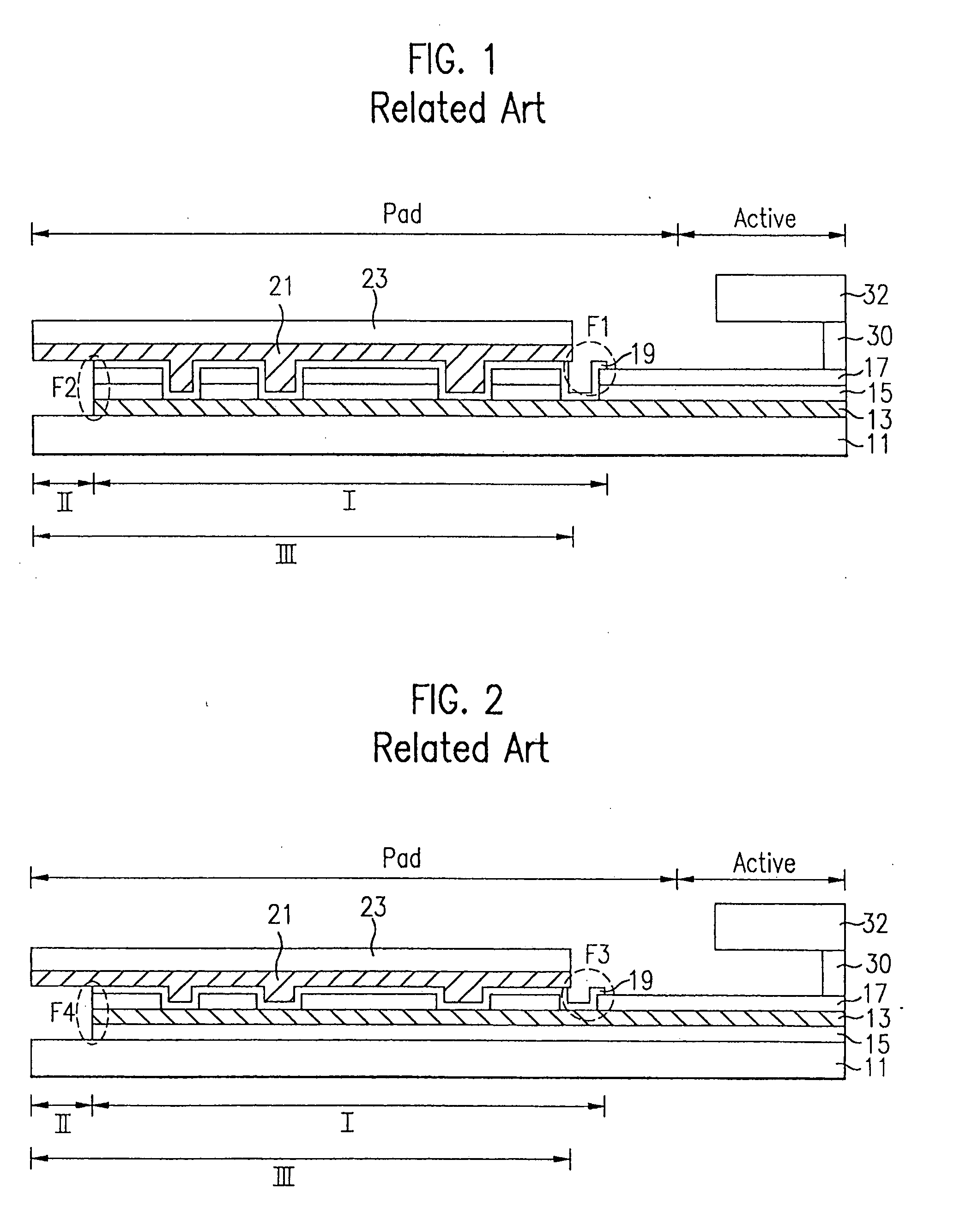
a liquid crystal display and pad technology, applied in the field of display devices, can solve the problems of increasing the possibility of atmospheric corrosion or electrolytic corrosion on a portion of the gate metal, conventional lcd pads are prone to atmospheric corrosion or electrolytic corrosion, and cannot meet the needs of electronic products with reduced size and weight, so as to prevent the properties of an lcd from being deteriorated

Inactive Publication Date: 2008-01-31
LG DISPLAY CO LTD
View PDF18 Cites 3 Cited by
  • Summary
  • Abstract
  • Description
  • Claims
  • Application Information

AI Technical Summary

Benefits of technology

[0022] An object of the present invention is to provide an LCD (Liquid Crystal Display) pad and a manufacturing method thereof, which can prevent properties of an LCD from being deteriorated by using improved gate and data pads sufficiently resistible against an electrolytic corrosion or a corrosion.

Problems solved by technology

However, conventional CRTs have not been able to respond to the need to manufacture electronic products with reduced size and weight because CRTs are fundamentally large and heavy.
For example, conventional LCD pads are prone to atmospheric corrosion or electrolytic corrosion.
If an electrical signal is applied to the gate pad to be operated, the sectional surfaces of the gate metal and the transparent metal layer exposed after the grinding process, or the portion of the transparent metal layer uncovered by the ACF may raise an electrochemical reaction which increases the possibility of atmospheric corrosion or electrolytic corrosion on a portion of the gate metal, thereby leading to damage of the gate pad.
That is, the thin film transistor is damaged due to a fine electrical shock generated during the electrochemical reaction, and the resistance of the gate wiring increases due to the atmospheric corrosion and the electrolytic corrosion of the gate metal.
If an electrical signal is applied to the data pad to be operated, an electrochemical reaction may be induced in the sectional surfaces of the source / drain metal and the transparent metal layer exposed after the grinding process or the portion of the transparent metal layer uncovered by the ACF which increases the possibility of atmospheric corrosion or electrolytic corrosion on a portion of the source / drain metal, thereby leading to damage of the data pad.
That is, the thin film transistor is damaged due to a fine electrical shock generated during the electrochemical reaction, and the resistance of the data wiring increases due to the atmospheric corrosion and the electrolytic corrosion of the source / drain metal.

Method used


Image

  • Pad structure for liquid crystal display and method of manufacturing thereof
  • Pad structure for liquid crystal display and method of manufacturing thereof
  • Pad structure for liquid crystal display and method of manufacturing thereof

Examples


Embodiment Construction

[0038] Reference will now be made in detail to the preferred embodiments of the present invention, examples of which are illustrated in the accompanying drawings.

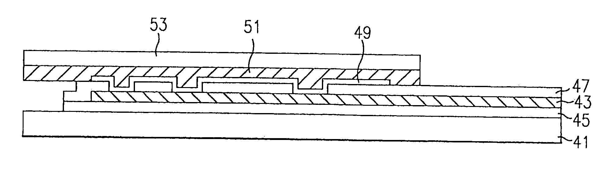
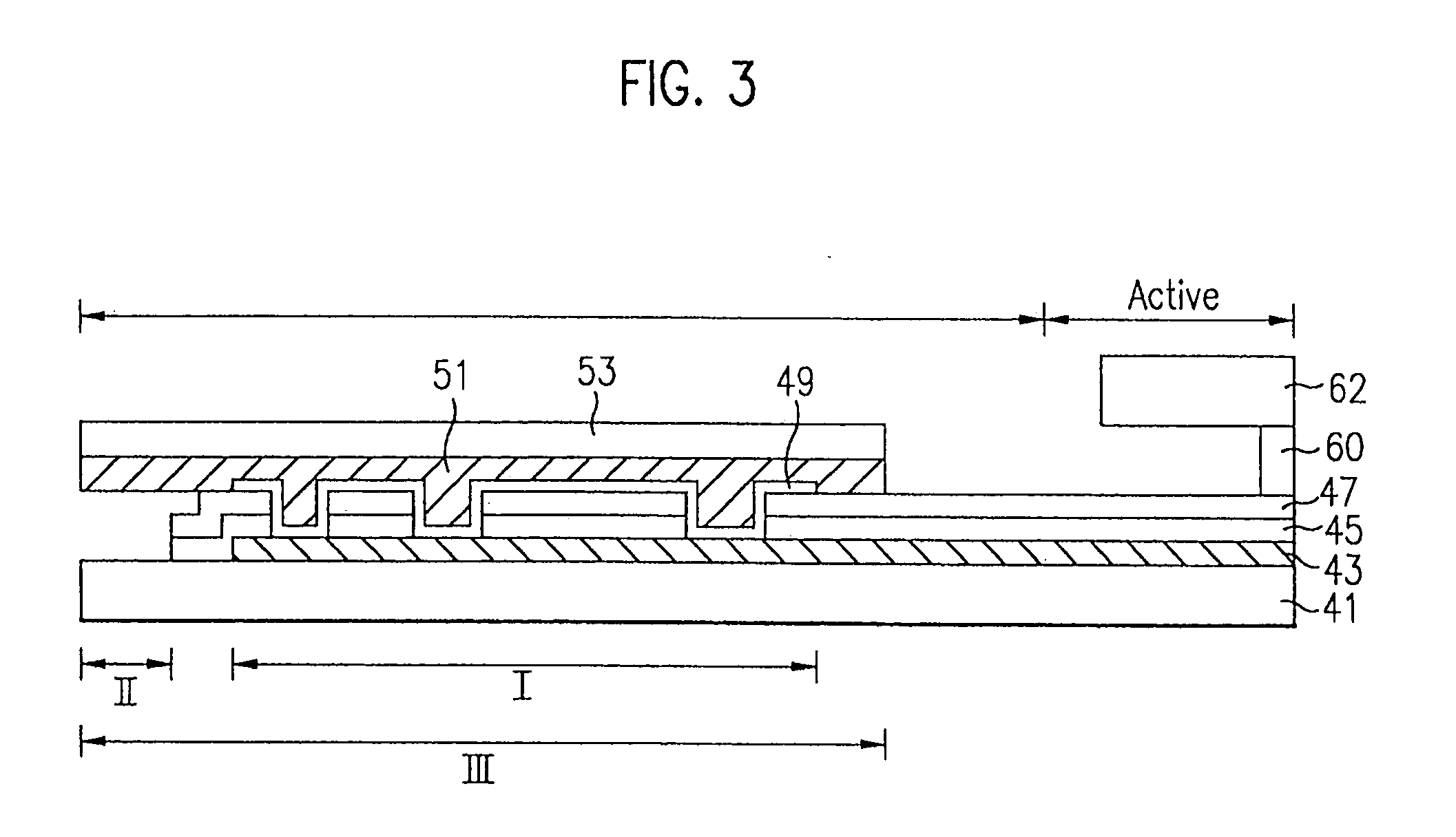
[0039] As will be explained in detail below, the gate and data pads and according to the present invention have contact holes formed within an ACF deposit area to transmit a gate signal and a data signal inputted from a TCP layer to a gate metal or a source / drain metal. Sectional surfaces of the transparent metal layer and the gate metal or the source / drain metal layer are protected from being exposed to ambient air after the grinding process, thereby preventing corrosion and / or electrolytic corrosion of the source / drain metal, the gate metal, or the transparent conductive layer.

[0040] Initially, a gate pad according to the present invention, as shown in FIG. 3 for example, is divided into an ACF (Anisotropic Conductive Film) deposit area III, a pad contact area I, and a grinding area II. Here, the pad contact area I is s...


PUM

PropertyMeasurementUnit
insulatingaaaaaaaaaa
transparentaaaaaaaaaa
conductiveaaaaaaaaaa

Abstract

A liquid crystal display has a pad structure. The pad structure includes at least one pad formed on a substrate, an insulating film formed on the pad, and at least one conductive layer connected to the pad through contact holes defined through the insulating film. The insulating film covers side surfaces of the pad and a portion of the substrate adjacent to the side surfaces of the pad.

Description

[0001] The present invention claims the benefit of Korean Patent Application No. 2000-43184 filed in Korea on Jul. 26, 2000, which is hereby incorporated by reference. BACKGROUND OF THE INVENTION [0002] 1. Field of the Invention [0003] The present invention generally relates to a display device and, more particularly, to pads for an LCD (Liquid Crystal Display) and a manufacturing method thereof. [0004] 2. Description of the Related Art [0005] CRTs (Cathode Ray Tubes) have been the primary type of display device for instrumentation system monitors, information system terminals, and televisions. However, conventional CRTs have not been able to respond to the need to manufacture electronic products with reduced size and weight because CRTs are fundamentally large and heavy. [0006] LCDs (Liquid Crystal Displays), which are relatively thin and light weight, have been developed to replace the conventional CRT. In recent years, LCDs have begun to play an important role as a plat-type disp...

Claims


Application Information

Patent Timeline
Patent Type & Authority Applications(United States)
IPC IPC(8): H01L21/44G02F1/13G02F1/1345G02F1/1362
CPCG02F1/1345G02F1/13458H05K1/112H05K2201/09509H05K3/361H05K2201/0326H05K2201/09436H05K3/323G02F1/13
Inventor YOO, SOON SUNGKWAK, DONG YEUNGKIM, HU SUNGKIM, YONG WANPARK, DUG JINJUNG, YU HOLEE, WOO CHAE
Owner LG DISPLAY CO LTD
Why Eureka
Try Eureka