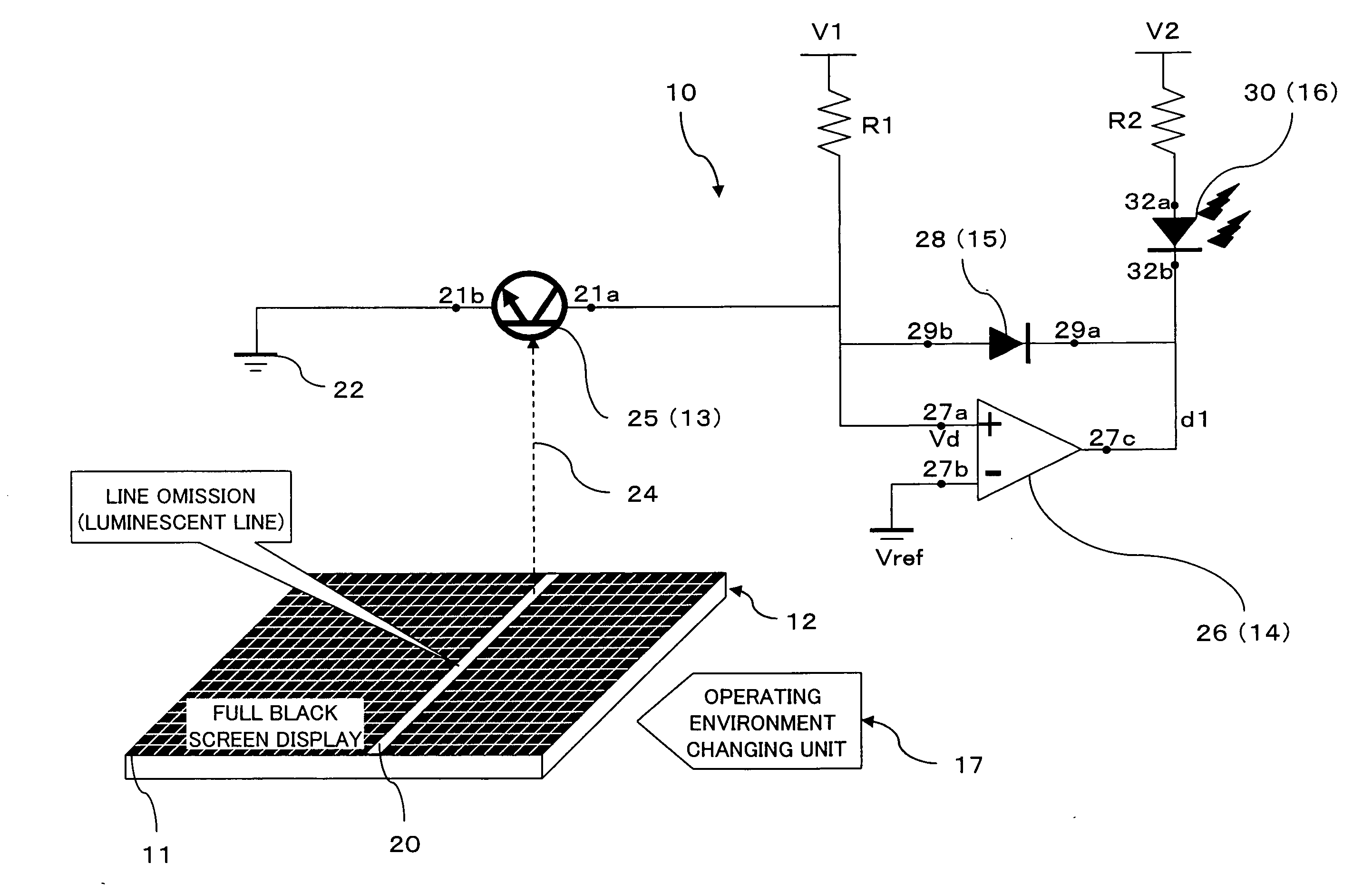
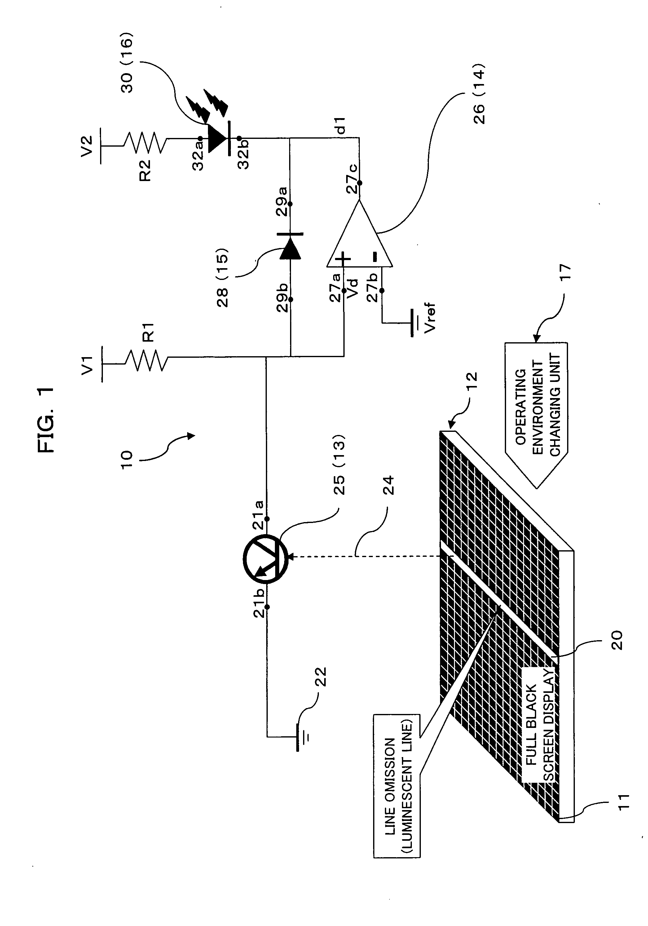
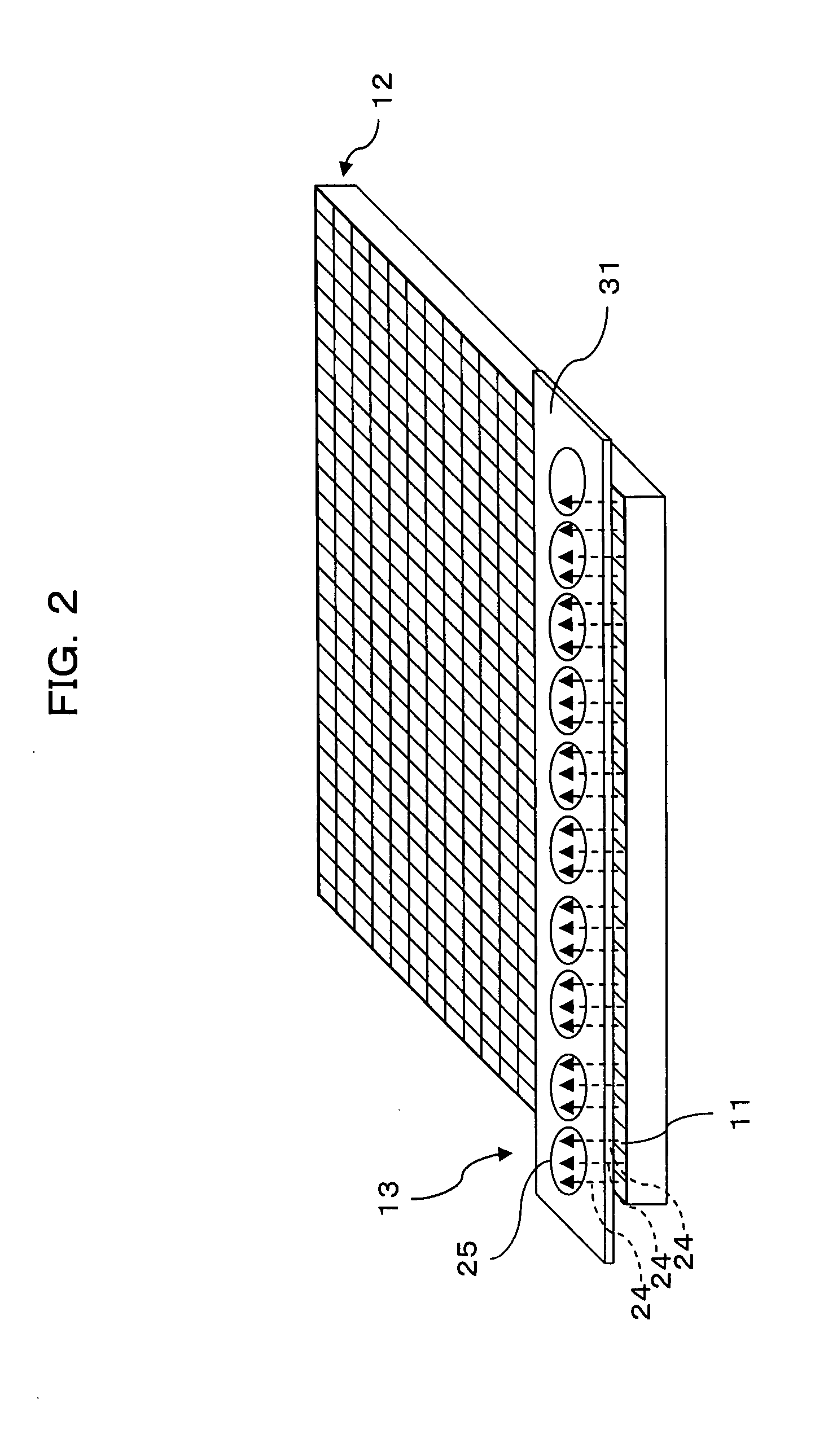
In addition, dot omission troubles due to the appearance of defective pixels in units of pixel and line omission troubles due to the continuous appearance of defective pixels in the form of a line are commonly known as such defective pixels of a display panel.
If a display panel contains defective pixels, the defective pixels cause defects such as difficulty of normal display and display of color different from intended color and, in this
manufacturing line, a display panel containing, for example, a certain proportion of defective pixels is handled as a defective product.
Such a very small number of defective pixels sprinkling in the display panel are not remarkable in use, and there is a tendency that a display panel having defective pixels smaller than a certain proportion of pixels is not handled as a defective product.
Meanwhile, since the line omission troubles are remarkable and frequently unsightly because defective pixels appear continuously in a display panel, it is preferred to detect the line omission troubles more effectively in comparison with the dot omission troubles.
Incidentally, such line omission troubles occur principally because foreign matters get mixed between electrodes of a display panel.
Moreover, the line omission trouble of the display panel also occurs due to, for example, the
thermal expansion of electrodes, insulating materials and foreign matters getting mixed into the display panel
stemming from an increase in temperature in the interior of the display panel, short circuits (semi-contact troubles) between electrodes arising in a case in which the display panel vibrates to move foreign matters therein, or disconnection or breaks (semi-disconnection troubles) of
electrode lines and, in many cases, for example, the semi-contact troubles or semi-disconnection troubles occur temporarily (in an instant) because of being involved in variations of
operating environment on the display panel such as variations in temperature in the interior of the display panel and vibrations of the display panel itself.
There is a problem which arises with the
conventional technique, however, in that difficulty is experienced in detecting the line omission troubles occurring temporarily.
For example, the technique of the above-mentioned
Patent Document 1 is made to only once pick up an image of the display screen and, hence, the non-occurrence of a semi-contact trouble or semi-disconnection trouble at the image
pickup makes it difficult to detect these troubles, which can cause a line omission trouble to occur during use afterwards even in a case in which no line omission trouble is detected by the inspection conducted when the display panel is put on the market from the factory.
In addition, in the case of the technique disclosed in the above-mentioned
Patent Document 1, if the image
pickup of the display screen is made more than once, the
inspection time to be taken for each display panel lengthens, which leads to incurring an increase in operator's burden or manufacturing cost.

