Photoelectric conversion device and image capturing device
- Summary
- Abstract
- Description
- Claims
- Application Information
AI Technical Summary
Benefits of technology
Problems solved by technology
Method used
Image
Examples
first embodiment
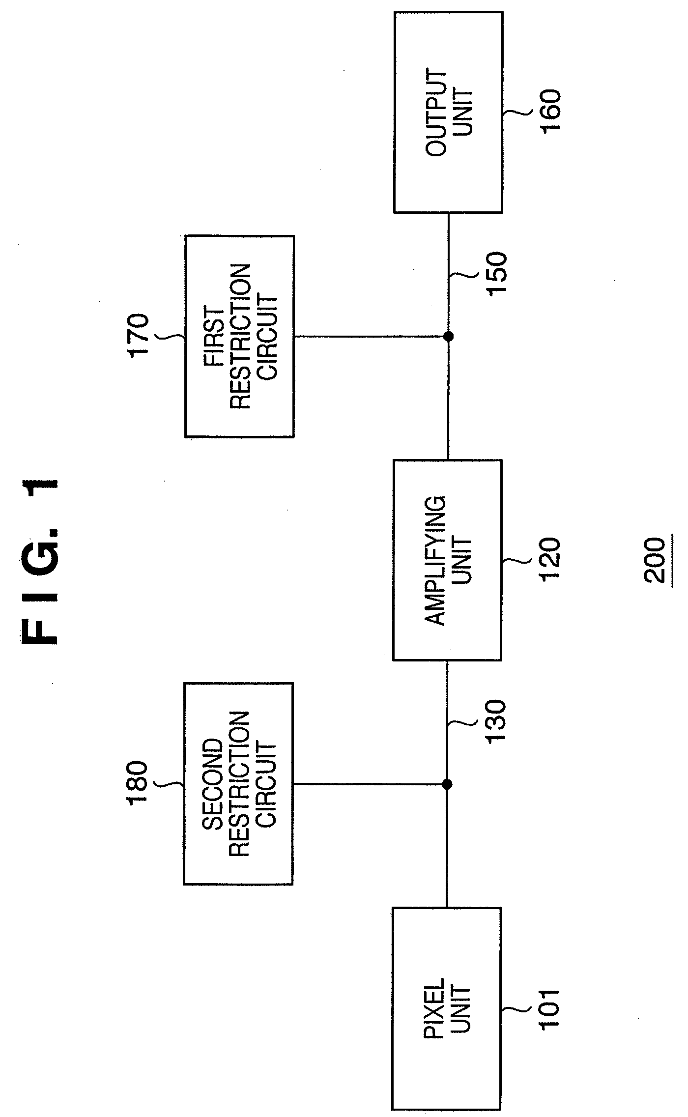
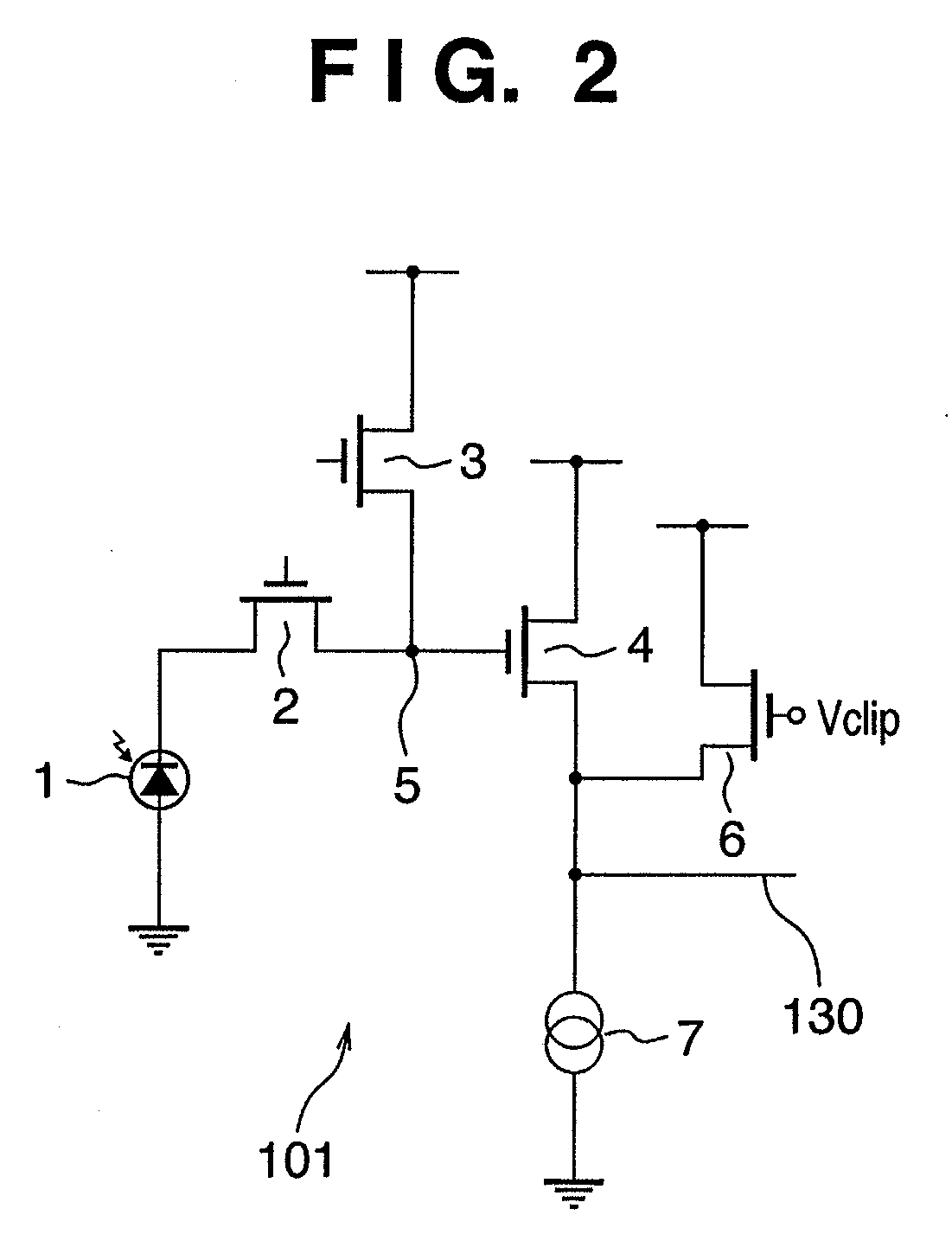
[0055]FIG. 3 is a circuit diagram showing the schematic arrangement of a photoelectric conversion device according to the first embodiment of the present invention. A photoelectric conversion device 210 shown in FIG. 3 is simplified, and its basic arrangement is the same as that of a photoelectric conversion device 100 shown in FIG. 11. A first clipping transistor 19 is an example of a first restriction circuit 170, and a second clipping transistor 6 is an example of a second restriction circuit 180.
[0056]FIG. 4 is a timing chart showing an example of a voltage change of the pixel output line when light of the first brightness (intermediate brightness) enters a pixel. FIG. 5 is a timing chart showing an example of a voltage change of the pixel output line when light of the second brightness (high brightness) enters a pixel. The operation of the photoelectric conversion device 210 shown in FIG. 3 will be explained with reference to FIGS. 4 and 5. Only the operation of a target readou...
second embodiment
[0070]FIG. 6 is a circuit diagram showing the schematic arrangement of a photoelectric conversion device according to the second embodiment of the present invention. A photoelectric conversion device 220 shown in FIG. 6 is simplified, and its basic arrangement is the same as that of a photoelectric conversion device 100 shown in FIG. 11. A transfer switch 16 functions as a first restriction circuit 170, and is controlled by the transfer pulse PH′ having the same logical level as the transfer pulse PH but the voltage level Vread different from the transfer pulse PH. A second clipping transistor 6 is an example of a second restriction circuit 180.
[0071]In the second embodiment, a noise level held by a capacitor 14 is clipped at a predetermined clip level (Vread−threshold) when provided to an output unit 160 including a differential amplifier via the transfer switch 16 functioning as the first restriction circuit 170. The second clipping transistor 6 has been described in the first emb...
third embodiment
[0073]FIG. 7 is a circuit diagram showing the schematic arrangement of a photoelectric conversion device according to the third embodiment of the present invention. A photoelectric conversion device 230 shown in FIG. 7 is simplified, and its basic arrangement is the same as that of a photoelectric conversion device 100 shown in FIG. 11. A transistor 19′ and a voltage detecting circuit 171 which controls it are an example of a first restriction circuit 170. A second clipping transistor 6 is an example of a second restriction circuit 180.
[0074]When the fluctuation width on a pixel output line 130 from the reset level falls within a specified width, the voltage detecting circuit 171 applies the voltage Vclip1 to the gate of the transistor 19′, similar to the first embodiment. If the fluctuation width on the pixel output line 130 from the reset level exceeds the specified width, the voltage detecting circuit 171 applies 0 V to the gate of the transistor 19′. As a result, the voltage of ...
PUM
 Abstract
Description
Claims
Application Information
 - R&D
- Intellectual Property
- Life Sciences
- Materials
- Tech Scout
- Unparalleled Data Quality
- Higher Quality Content
- 60% Fewer Hallucinations
Browse by: Latest US Patents, China's latest patents, Technical Efficacy Thesaurus, Application Domain, Technology Topic, Popular Technical Reports.
© 2025 PatSnap. All rights reserved.Legal|Privacy policy|Modern Slavery Act Transparency Statement|Sitemap|About US| Contact US: help@patsnap.com


