Fabricating method of plastic substrate

a technology of plastic substrate and fabrication method, which is applied in the direction of superimposed coating process, liquid/solution decomposition chemical coating, instruments, etc., can solve the problems of increasing the manufacturing cost of the display device, the limitation of the application and use of flat-panel display devices, and the high cost of flexible substrates, etc., to improve the stability of the display device fabrication process, the effect of easy to obtain and cheapness

Active Publication Date: 2008-02-14
LG DISPLAY CO LTD
View PDF3 Cites 8 Cited by
  • Summary
  • Abstract
  • Description
  • Claims
  • Application Information

AI Technical Summary

Benefits of technology

[0019]An advantage of the present invention is to provide a fabricating method of a plastic substrate adapted to improve the stability of a display device fabrication process. The fabrication process utilizes the plastic substrate, which is inexpensive and easy to obtain.
[0020]Additional features and advantages of the invention will be set forth in the description which follows, and in part will be apparent from the description, or may be learned by practice of the invention. These and other advantages of the invention will be realized and attained by the method particularly pointed out in the written description and claims hereof as well as the appended drawings.
[0021]To achieve these and other advantages and in accordance with the purpose of the present invention, as embodied and broadly described, a fabricating method includes providing a plastic substrate; spreading an organic film on the plastic substrate; and applying heat to the plastic substrate over which the organic film is spread to conduct heat to the plastic substrate and to harden the organic film at the same time.
[0022]In another aspect of the present invention, a fabricating method includes providing a deformed plastic substrate having heat directivity; spreading an organic film on the plastic substrate; and applying heat to the plastic substrate over which the organic film is spread to conduct heat to the plastic substrate and to harden the organic film at the same time.
[0023]It is to be understood that both the foregoing general description and the following detailed description are exemplary and explanatory and are intended to provide further explanation of the invention as claimed.

Problems solved by technology

However, because glass substrates are not flexible, there is a limit in the application and use of flat panel display devices.
However, utilizing PES as the material for the flexible substrate becomes very expensive, thereby increasing manufacturing costs of the display device.
That is, the PES substrate is an expensive plastic material.
Thus, it is difficult to properly form a wire line in the array process because a PEN plastic substrate is non-uniform and deformed by heat generated during the process that causes the above mentioned directivity.
That is, an inexpensive plastic, such as PEN, obtains a non-uniform surface roughness during an initial heat process.
This causes difficulty in correctly forming a wire line in the subsequent array process.
As a result, it is difficult to carry out a stable array process on plastics substrates made of materials other than PES.
That is, it is difficult to carry out a stable array process on a plastic substrate, such as PEN, which is inexpensive and easy to fabricate.

Method used


Image

  • Fabricating method of plastic substrate
  • Fabricating method of plastic substrate
  • Fabricating method of plastic substrate

Examples


Embodiment Construction

[0032]Reference will now be made in detail to the embodiments of the present invention, examples of which are illustrated in the accompanying drawings.

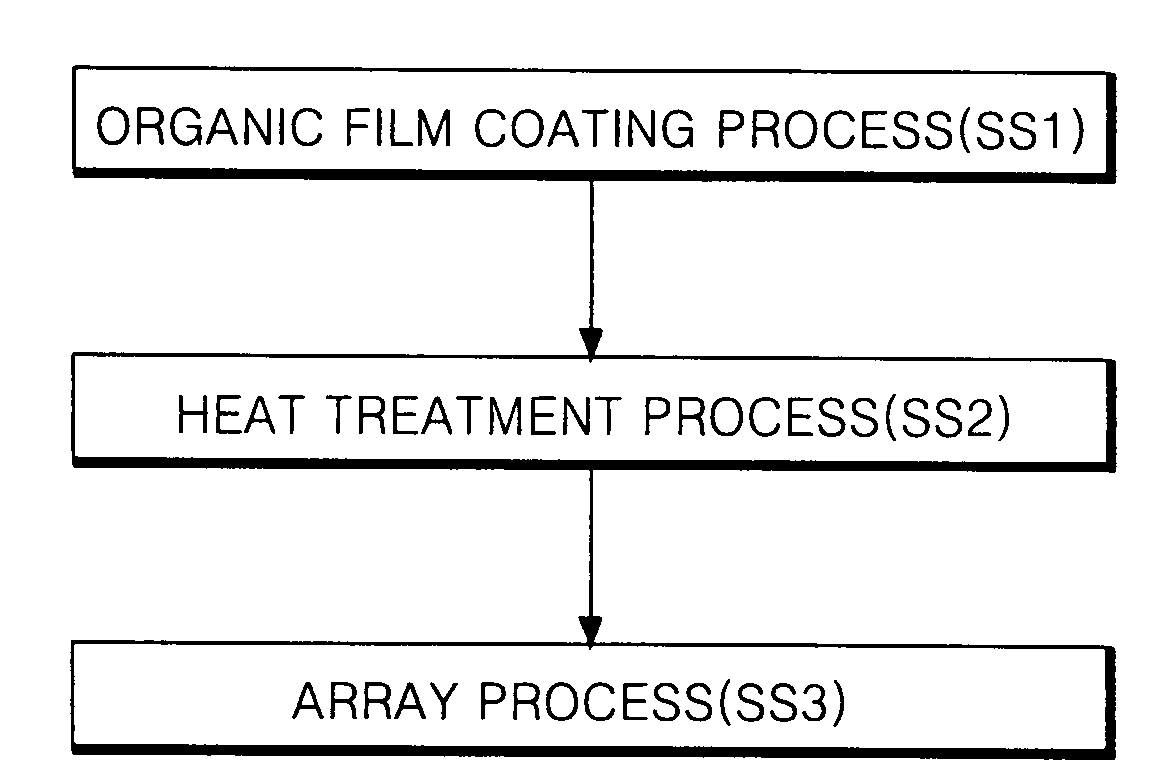
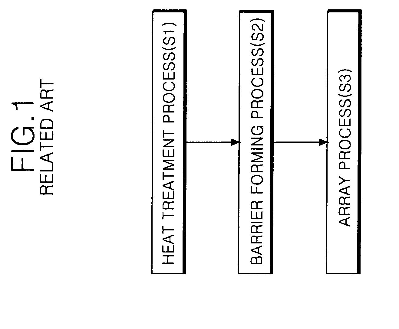
[0033]FIG. 3 is a diagram for explaining a fabricating method of a TFT array substrate using a flexible plastic substrate according to an embodiment of the present invention.

[0034]In an embodiment of the present invention, low cost plastic materials that have been deformed with directivity using a heat treatment are employed. That is, low cost plastic materials that have been deformed in one-direction in which heat is applied are utilized. These materials include, for example, polyethylene naphthalate (PEN), polyethylene terephthalate (PET) and polycarbonate (PC). These materials are advantageous in that they are inexpensive and easy to manufacture.

[0035]The plastic materials according to the above-mentioned embodiment of the present invention have a non-uniform surface, thus the surface should be made even so as for wire lines of a d...


PUM


Abstract

This invention relates to a fabricating method of a plastic substrate adapted to improve the stability of a display device fabrication process. The fabrication process utilizes the plastic substrate, which is inexpensive and easy to obtain. A fabricating method according to an embodiment of the present invention includes providing a plastic substrate; spreading an organic film on the plastic substrate; and applying heat to the plastic substrate over which the organic film is spread to conduct heat to the plastic substrate and to harden the organic film at the same time.

Description

[0001]This application claims the benefit of Korean Patent Application No. P06-0042892 filed on May 12, 2006, which is hereby incorporated by reference for all purposes as if fully set forth herein.BACKGROUND OF THE INVENTION[0002]1. Field of the Invention[0003]The present invention relates to a substrate for a display device. More particularly, the present invention relates to a fabricating method of a plastic substrate adapted to improve the stability of a display device fabrication process. The fabrication process utilizes the plastic substrate, which is inexpensive and easy to obtain.[0004]2. Description of the Related Art[0005]Recently, the display device market has focused its attention on flat panel display devices because these devices are easily manufactured to be thin, light and large-sized.[0006]Flat panel display devices include, for example, liquid crystal display (LCD) devices, plasma display panels (PDP), and organic electro luminescence displays (OLED). These flat pa...

Claims


Application Information

Patent Timeline
Patent Type & Authority Applications(United States)
IPC IPC(8): B05D5/00
CPCG02F1/133305H01L51/0097Y02E10/549H01L2251/5338H01L51/52H10K77/111H10K50/80H10K2102/311G02F1/1333
Inventor LEE, KYOUNG MOOKKIM, SUNG HWAN
Owner LG DISPLAY CO LTD
Why Eureka
Try Eureka