Patterning of solid state features by direct write nanolithographic printing

a nanolithographic printing and solid state feature technology, applied in the field of direct write nanolithographic printing, can solve the problems of short circuit, large problems of the prior art lithographic method for making nanoscale solid state features that are generally limited to scales larger, and can generate significant problems in the miniaturization of electronic and optical devices, etc., to achieve fast patterning by dpn printing, large surface area, and low cost

Inactive Publication Date: 2008-02-21
NORTHWESTERN UNIV
View PDF5 Cites 5 Cited by
  • Summary
  • Abstract
  • Description
  • Claims
  • Application Information

AI Technical Summary

Benefits of technology

[0019] Basic and novel features of the invention are set forth below and include, for example, direct write capability, serial patterning with ultrahigh resolution, molecular generality and use of wide variety of functional groups and materials, relatively low cost, ease of use, non-planar substrates, and unparalleled registration. The invention, briefly, opens up the opportunity for using DPN printing to deposit solid-state materials rather than organic molecules onto surfaces with the resolution of an AFM without the need for a driving force other than chemisorption such as, for example, applied fields. The invention can be used in areas ranging from mask fabrication to the evaluation of solid-state nanoelectronic structures and devices fabricated by DPN printing. Because the diffusion coefficients of sol inks are qualitatively comparable to that of alkanethiols on gold, relatively fast patterning by DPN printing can be carried out. The composite nanostructures described herein can have large surface areas that are important for catalyst and wave-guide applications. Use of complicated and expensive resists, photomasks, and molds are not needed.

Problems solved by technology

However, attempted miniaturization in making electronic and optical devices can generate significant problems.
For example, failure to provide adequate separation between electrical current carrying features may lead to short circuiting.
The prior art lithographic methods for making nanoscale solid state features are generally limited to scales larger than nanoscopic.

Method used


Image

  • Patterning of solid state features by direct write nanolithographic printing
  • Patterning of solid state features by direct write nanolithographic printing
  • Patterning of solid state features by direct write nanolithographic printing

Examples


working examples

Experimental

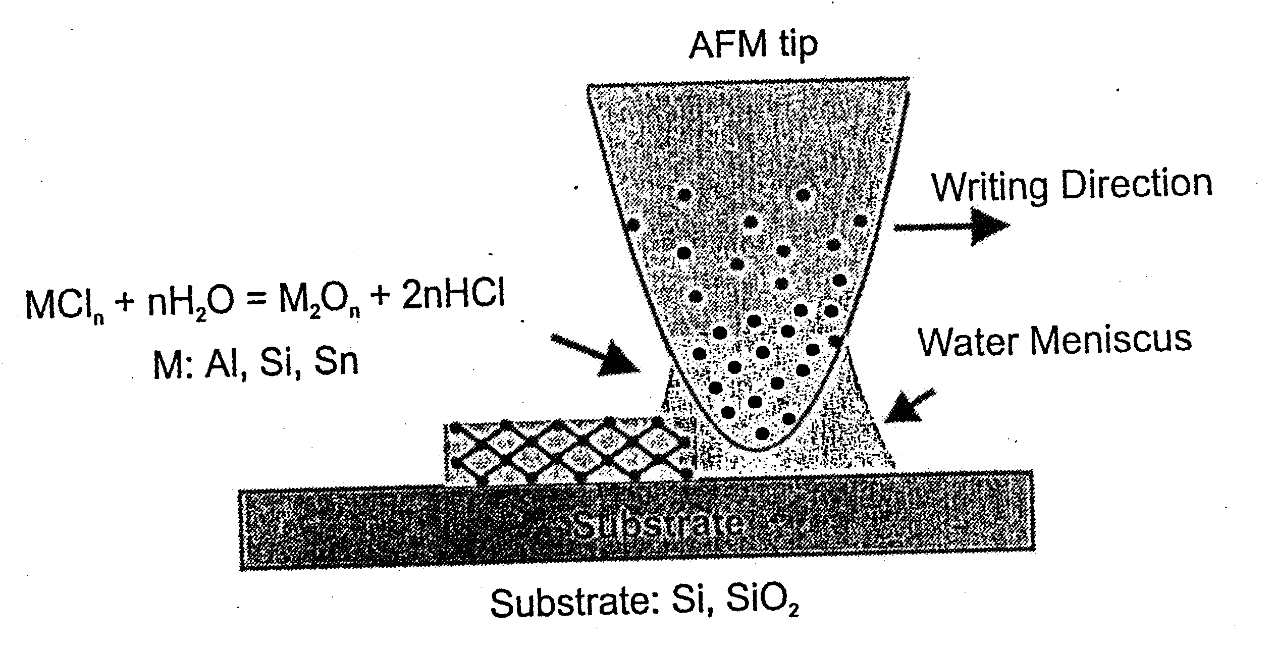
[0083] A ThermoMicroscopes CP AFM and conventional silicon nitride micro-cantilevers (force constant of 0.05 N / m) were used for all patterning experiments. In each experiment, the tip was coated by dipping it into the as-prepared sols at room temperature for 20 seconds. All patterning experiments were conducted under ambient conditions without rigorous control over humidity (˜40%) and temperature (˜20° C.) with a tip-surface contact force of 0.5 nN. To minimize the piezo tube drift, a 90 μM scanner with closed loop scan control was used for all patterning experiments. Subsequent imaging of the generated patterns was done with the ink-coated tip under conditions identical to those used for patterning but at a higher scan rate (6 Hz).

[0084] In a typical experiment, an inorganic precursor solution (sol) was prepared by dissolving 1 g of the block copolymer poly (ethyleneoxide)-b-poly (propyleneoxide)-b-poly (ethyleneoxide), (EO20PO70EO20) (Pluronic P-123, BASF) in 10 g of...

examples 1 and 2

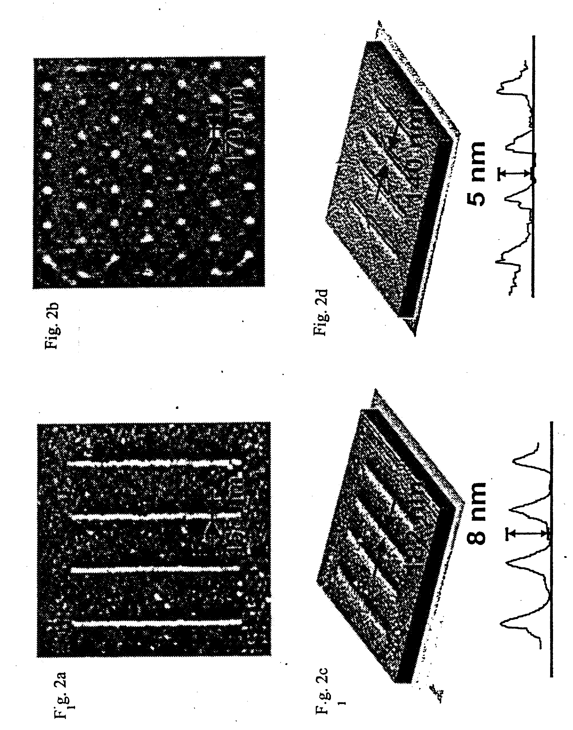
[0085] Dots, lines and complex patterns comprised of tin-oxide and aluminum oxide have been generated on silicon and silicon oxide (>600 nm oxidation layer) substrates, as shown in FIG. 2. For example, 155 nm wide parallel lines made of tin-oxide have been constructed on SiO2 by moving a tip coated with the composite ink (SnCl4 and P-123) across the substrate (0.2 μm / sec). Similarly, dots consisting of Al2O3 were generated on a Si substrate using a tip coated with (AlCl3 and P-123) by successively bringing the tip in contact with substrate for 1 s / dot intervals. These structures maintain their shapes even after repeated imaging (5 times) and are indefinitely stable (>1 month) under ambient conditions.

example 3

[0086] A Si sol (comprised of SiCl4 and P-123) was patterned onto a silicon oxide substrate in the form of parallel lines. The composition of the lines is expected to be a mixture of SiOx and the polymer. When heated in air at 400° C. for 2 hour, the copolymer surfactant is expected to combust leaving a SiO2 nanostructure. Consistent with this hypothesis, an AFM image collected from the same area post heating indicated that the pattern height decreases from 8 nm to 5 nm, FIGS. 2c and 2d.


PUM

PropertyMeasurementUnit
speedaaaaaaaaaa
holding timeaaaaaaaaaa
temperatureaaaaaaaaaa

Abstract

The present invention includes a method of fabricating organic / inorganic composite nanostructures on a substrate comprising depositing a solution having a block copolymer and an inorganic precursor on the substrate using dip pen nanolithography. The nanostructures comprises arrays of lines and / or dots having widths / diameters less than 1 micron. The present invention also includes a device comprising an organic / inorganic composite nanoscale region chemically bonded to a substrate, wherein the nanoscale region, wherein the nanoscale region has a nanometer scale dimension other than height.

Description

CROSS-REFERENCE TO RELATED PATENT APPLICATIONS [0001] This application claims benefit of provisional application 60 / 341,614, filed Dec. 17, 2001, the complete disclosure of which is incorporated herein by reference in its entirety.[0002] This invention was made with governmental support under grant ______. The government has certain rights in the invention.BACKGROUND OF THE INVENTION [0003] DIP-PEN NANOLITHOGRAPHY™ printing (DPN™ printing) is a high resolution direct patterning technique in which an “ink” is transferred to a substrate using conventional nanoscopic tips including, for example, scanning probe microscopic (SPM) and atomic force microscopic (AFM) tips. See, e.g., U.S. patent application Ser. Nos. 60 / 115,133, filed Jan. 7, 1999; 60 / 157,633, filed Oct. 4, 1999; 09 / 477,997, filed Jan. 5, 2000; 60 / 207,711, filed May 26, 2000; 60 / 207,713, filed May 26, 2000; 09 / 866,533, filed May 24, 2001; and 60 / 326,767, filed Oct. 2, 2001, and PCT applications numbers PCT / US00 / 00319, filed...

Claims


Application Information

Patent Timeline
Patent Type & Authority Applications(United States)
IPC IPC(8): B05D5/00B82B3/00G03F7/00H01L21/027
CPCB82B3/00B82Y10/00B82Y30/00B82Y40/00Y10T428/24926Y10S977/857Y10S977/855Y10T428/24802Y10T428/265G03F7/0002G03F7/00
Inventor MIRKIN, CHADADRAVID, VINAYAK P.SU, MINGLIU, XIAOGANG
Owner NORTHWESTERN UNIV
Why Eureka
Try Eureka