Differential circuit and output buffer circuit including the same

a technology of differential circuit and output buffer, which is applied in the direction of pulse generator, pulse technique, field effect transistor reliability increase, etc., can solve the problems of deteriorating reliability of thin gate oxide transistor, inability to provide high output voltage at output buffer using conventional cmos circuit, and inability to provide high operational speed of thick gate oxide transistor

Inactive Publication Date: 2008-02-28
SAMSUNG ELECTRONICS CO LTD
View PDF5 Cites 33 Cited by
  • Summary
  • Abstract
  • Description
  • Claims
  • Application Information

AI Technical Summary

Benefits of technology

[0051]Therefore, the output buffer circuit is capable of providing simultaneously both of the high operational speed and the high-voltage output signal.

Problems solved by technology

Accordingly, it is more difficult to provide a high output voltage at an output buffer using a conventional CMOS circuit.
Thus, a voltage difference between the gate and the body of each of the transistors NT11 and NT12 can be larger than the maximum allowable voltage of 1.2 volts of the low-voltage gate oxide NMOS transistor, and thus reliability of the thin gate oxide can be deteriorated.
The thick gate oxide transistor cannot provide high operational speed due to relatively low driving capacity, compared with the thin gate oxide transistor.
However, the reliability of the low-voltage gate oxide transistor can be deteriorated due to a bias voltage higher than the maximum allowable voltage of the low-voltage gate oxide transistor.
Thus, it is difficult to employ the low-voltage gate oxide transistor in an output buffer circuit that operates at a high power supply voltage.
Therefore, the conventional output buffer circuit that operates at the high power supply voltage so as to obtain the high-voltage output signal cannot provide the high operational reliability and the high operational speed at the same time.
That is, the conventional output buffer circuit that operates at the high power supply voltage cannot simultaneously provide both the high operational speed and the high-voltage output signal.

Method used


Image

  • Differential circuit and output buffer circuit including the same
  • Differential circuit and output buffer circuit including the same
  • Differential circuit and output buffer circuit including the same

Examples


Embodiment Construction

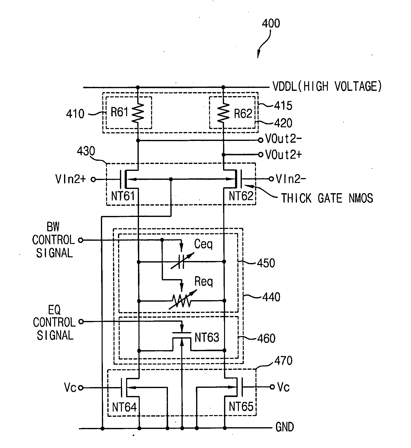
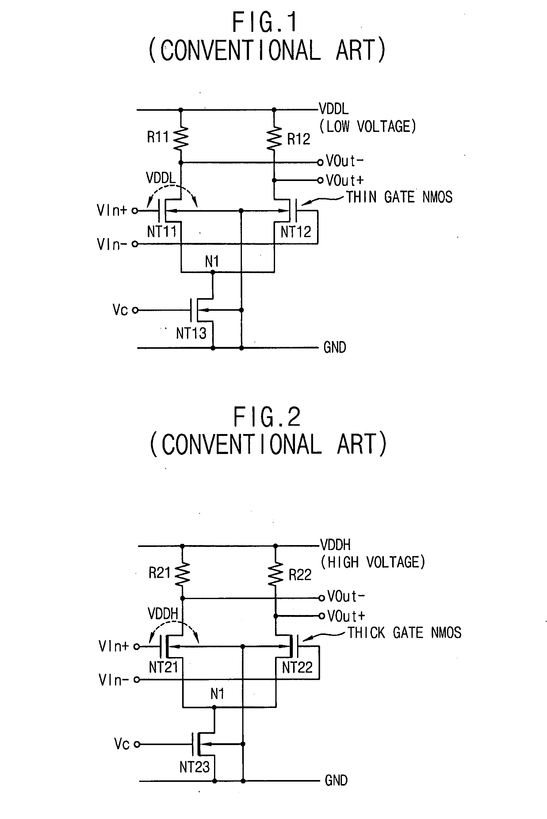
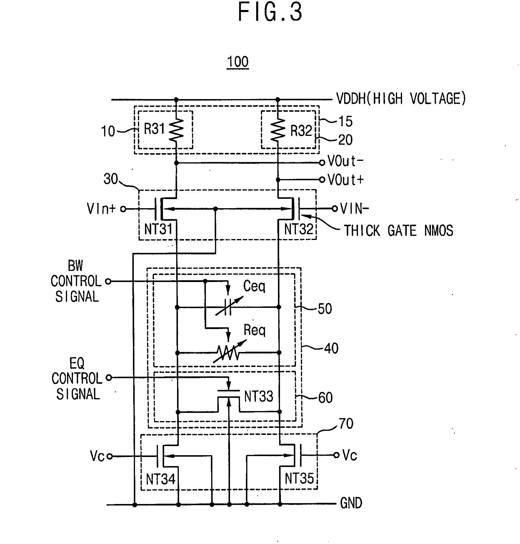
[0061]Embodiments of the present invention now will be described more fully with reference to the accompanying drawings, in which embodiments of the invention are shown. The present invention can, however, be embodied in many different forms and should not be construed as limited to the embodiments set forth herein. Rather, these embodiments are provided so that this disclosure will be thorough and complete, and will fully convey the scope of the invention to those skilled in the art. Like reference numerals refer to like elements throughout this application.

[0062]It will be understood that, although the terms first, second, etc. can be used herein to describe various elements, these elements should not be limited by these terms. These terms are used to distinguish one element from another. For example, a first element could be termed a second element, and, similarly, a second element could be termed a first element, without departing from the scope of the present invention. As used...


PUM


Abstract

An output buffer circuit in a multi-power system operating at a high power supply voltage and a low power supply voltage includes a pre-driver, and a main driver. The pre-driver performs a differential switching operation on first and second differential input signals to output first and second differential output signals. The main driver performs a differential switching operation on the DC-eliminated and level-shifted first and second differential output signals to output third and fourth differential output signals. The main driver includes a differential switching circuit including first and second NMOS transistors, and performs a differential switching operation on the DC-eliminated and level-shifted first and second differential output signals to output the third and fourth differential output signals, and an equalizer coupled between source electrodes of the first and second NMOS transistors, and controls a bandwidth of the third and fourth differential output signals.

Description

CROSS-REFERENCE TO RELATED APPLICATIONS[0001]This application claims priority under 35 USC § 119 to Korean Patent Application No. 10-2006-0068839, filed on Jul. 24, 2006 in the Korean Intellectual Property Office (KIPO), the disclosure of which is incorporated herein in its entirety by reference.BACKGROUND OF THE INVENTION[0002]1. Field of the Invention[0003]The present invention relates to a power supply in a semiconductor memory device, and more particularly to a differential circuit and an output buffer including the differential circuit.[0004]2. Description of the Related Art[0005]A power supply voltage used in a complementary metal-oxide semiconductor (CMOS) circuit has been decreasing according to the development of CMOS technology. Accordingly, it is more difficult to provide a high output voltage at an output buffer using a conventional CMOS circuit.[0006]FIG. 1 is a circuit diagram illustrating a conventional output buffer employing a transistor having a low-voltage gate ox...

Claims


Application Information

Patent Timeline
Patent Type & Authority Applications(United States)
IPC IPC(8): H03B1/00
CPCH03F3/45183H03K19/018564H03F3/45475H03F3/45632H03F3/45928H03F2200/168H03F2200/411H03F2203/45101H03F2203/45138H03F2203/45354H03F2203/45458H03F2203/45482H03F2203/45494H03F2203/45652H03K19/00315H03F3/45197H01L27/06
Inventor RUY, JONG-JAE
Owner SAMSUNG ELECTRONICS CO LTD
Why Eureka
Try Eureka