Modular command structure for memory and memory system

Active Publication Date: 2008-02-28
MOSAID TECH
View PDF21 Cites 98 Cited by
  • Summary
  • Abstract
  • Description
  • Claims
  • Application Information

AI Technical Summary

Benefits of technology

[0009]In accordance with another aspect of the present invention, there is provided A method of requesting access to at least one memory device, the method comprising: determining an address including an address for the at lest one memory device; identifying a plurality of operations that in combination effect a request for access

Problems solved by technology

If the individual memory devices are serially interconnected in a chain configuration with only one memory device connected to the controller, then commands for memory devices located later in the chain may be significantly delayed by earlier memory devices performing

Method used


Image

  • Modular command structure for memory and memory system
  • Modular command structure for memory and memory system
  • Modular command structure for memory and memory system

Examples


Embodiment Construction

[0049]In the following detailed description of sample embodiments, reference is made to the accompanying drawings which form a part hereof, and in which is shown by way of illustration specific sample embodiments. These embodiments are described in sufficient detail to enable those skilled in the art to practice the present invention, and it is to be understood that other embodiments may be used and that logical, mechanical, electrical and other changes may be made without departing from the scope of the present invention. Therefore, the following detailed description is not to be taken in a limiting sense.

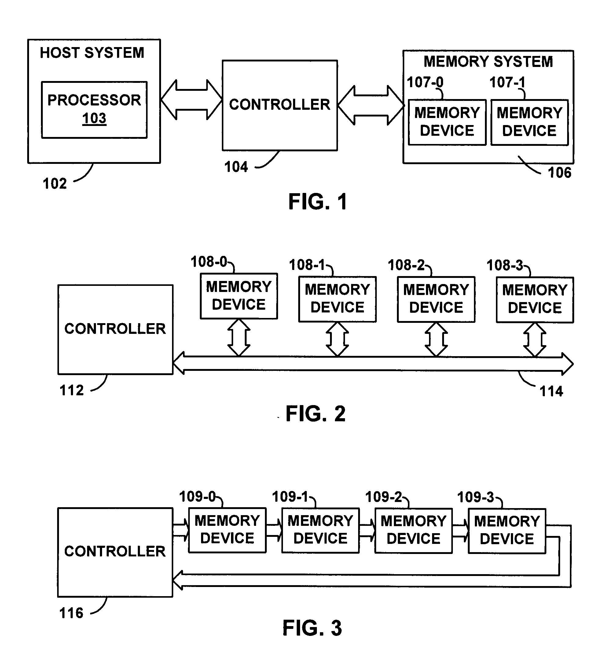
[0050]Semiconductor memory devices are often interconnected to form a large capacity memory system. FIG. 1 illustrates a system to which embodiments of the present invention are applicable. Referring to FIG. 1, a host system 102 having a processor 103 therein is connected to a system that includes a memory system 106 and a controller 104 for controlling the memory system. The memo...


PUM


Abstract

A system including a memory system and a memory controller is connected to a host system. The memory system has at least one memory device storing data. The controller translates the requests from the host system to one or more separatable commands interpretable by the at least one memory device. Each command has a modular structure including an address identifier for one of the at least one memory devices and a command identifier representing an operation to be performed by the one of the at least one memory devices. The at least one memory device and the controller are in a series-connection configuration for communication such that only one memory device is in communication with the controller for input into the memory system. The memory system can include a plurality of memory devices connected to a common bus.

Description

CROSS REFERENCE TO RELATED APPLICATIONS[0001]This application claims the benefit of priority of U.S. Provisional Patent Application No. 60 / 839,329 filed Aug. 22, 2006, U.S. Provisional Patent Application No. 60 / 902,003 filed Feb. 16, 2007, and U.S. Provisional Patent Application No. 60 / 892,705 filed Mar. 2, 2007, the disclosures of which are expressly incorporated herein by reference in their entirety.FIELD OF THE INVENTION[0002]The present invention relates generally to semiconductor memory devices and in particular to a system having multiple interconnected semiconductor memory devices and command structure for memory devices.BACKGROUND OF THE INVENTION[0003]Semiconductor memory devices are commonly found in many industrial and consumer electronics products. An increasing demand for higher memory capacity coupled with a requirement for smaller sizes results in a desire for memory with a density that is difficult to attain. As a result, multiple memory devices are often connected t...

Claims


Application Information

Patent Timeline
IPC IPC(8): G06F12/06G06F12/00
CPCG06F13/1678Y02B60/1228G11C7/1045G11C7/10Y02D10/00G11C7/22
Inventor KIM, JIN-KIOH, HAKJUNEPYEON, HONG BEOM
Owner MOSAID TECH
Why Eureka
Try Eureka