Scan chain in a custom electronic circuit design

a custom electronic circuit and scan chain technology, applied in computer aided design, instruments, pulse techniques, etc., can solve the problems of inability to separate multiple instances of similar or identical logic, less productivity than that of a designer using cell-based methodologies, and irregular fractions of logi

Inactive Publication Date: 2008-03-06
IBM CORP
View PDF3 Cites 0 Cited by
  • Summary
  • Abstract
  • Description
  • Claims
  • Application Information

AI Technical Summary

Benefits of technology

[0018]The propagation of scan inputs and scan outputs to the top level allows the determination of the position of all storage elements without analyzing each relevant sub-cell and without substantial calculations.

Problems solved by technology

Computer-aided design tools do not always provide the flexibility to allow the designer enough control to arrive at the optimal solution.
Accordingly, a significant amount of custom electronic circuit design tends to be manually driven, resulting in far less productivity than that of a designer using a cell-based methodology.
For example, in a processor design a large fraction of the logic is irregular and cannot be separated into multiple instances of similar or identical logic.

Method used


Image

  • Scan chain in a custom electronic circuit design
  • Scan chain in a custom electronic circuit design
  • Scan chain in a custom electronic circuit design

Examples


Embodiment Construction

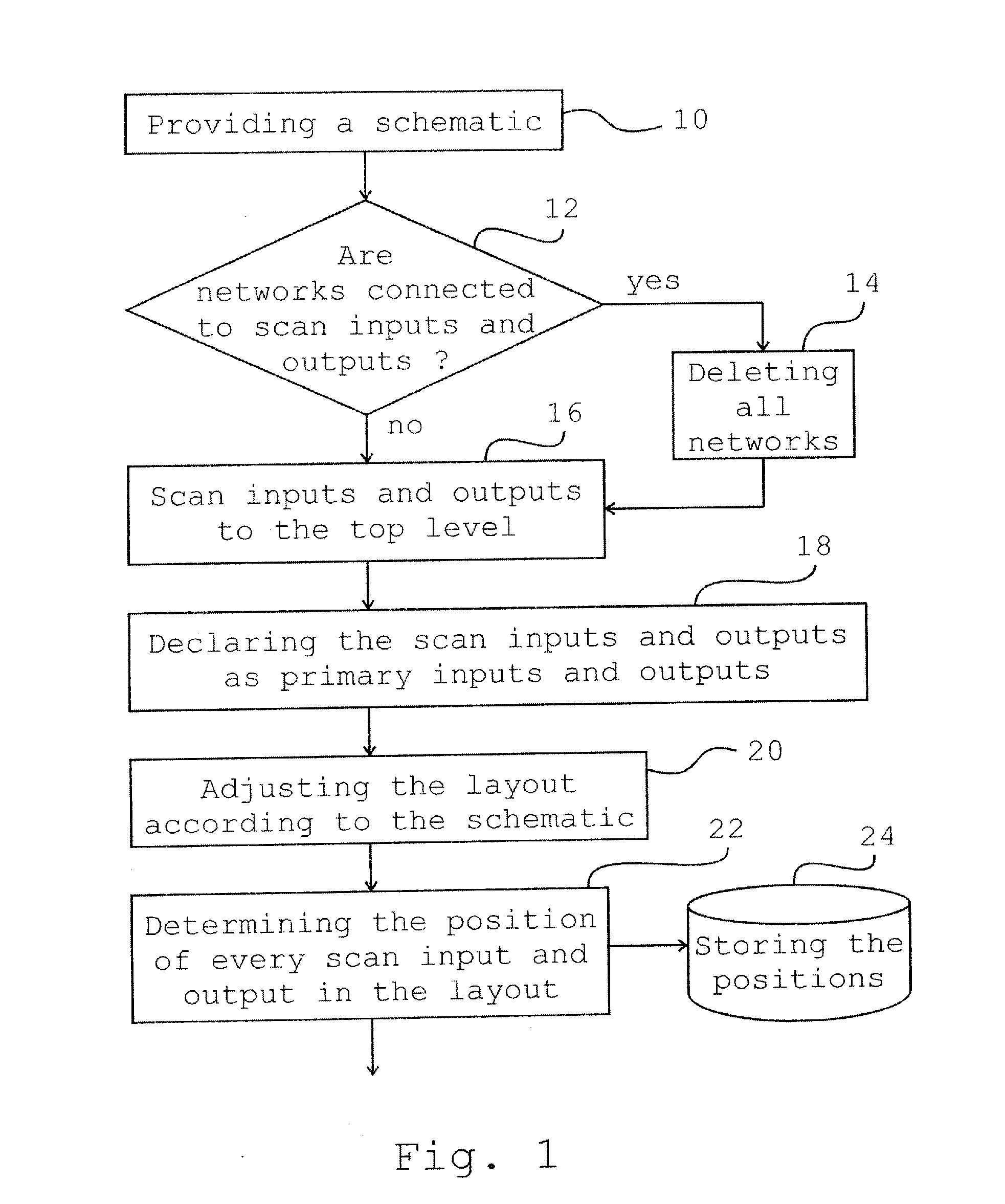
[0026]FIG. 1 shows a flow chart diagram that illustrates a first part of a method of using the scan chain cell design structure according to a preferred embodiment the present invention.

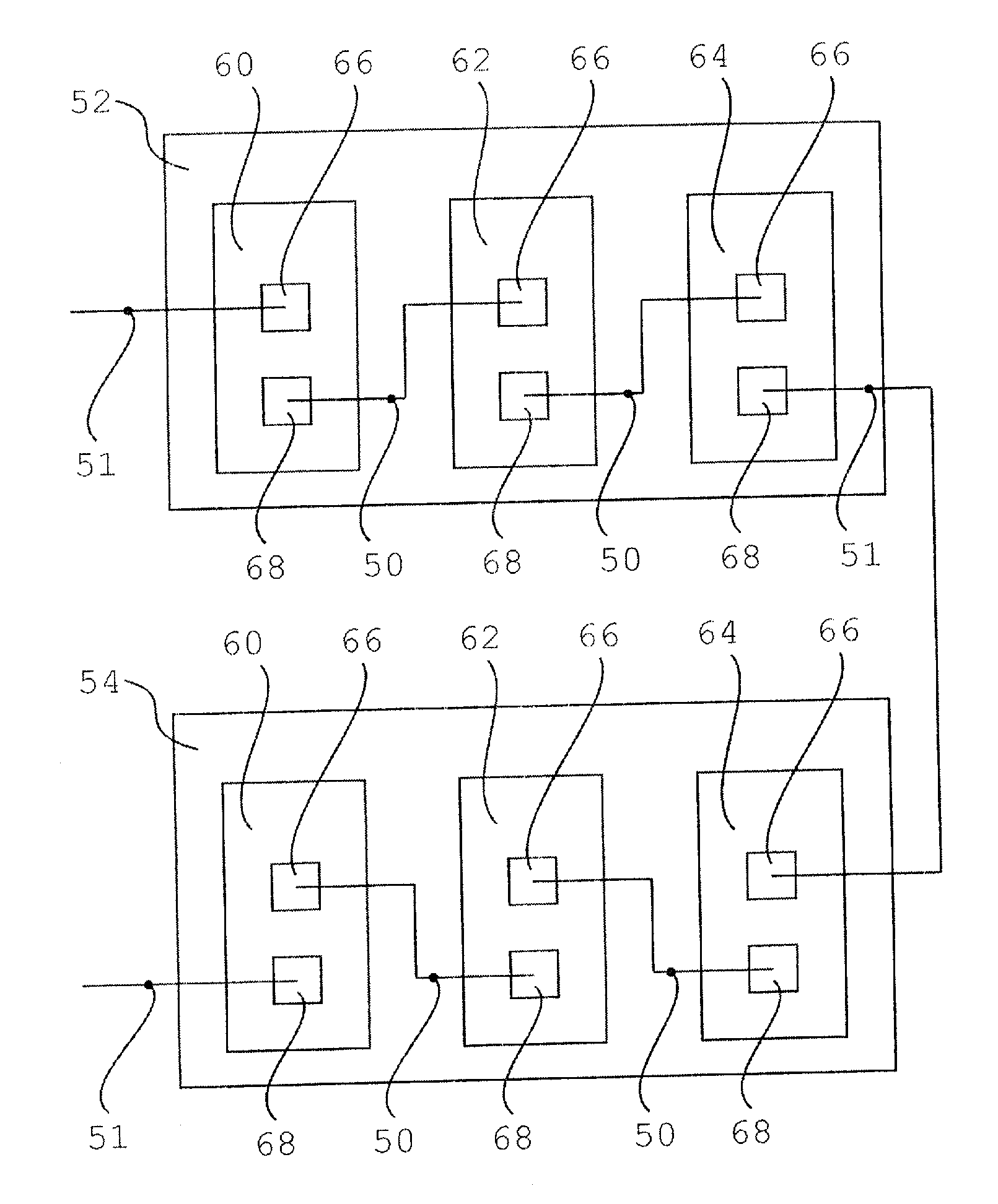
[0027]In a step 10 a schematic of a custom circuit is provided. The schematic is a structural description of said custom circuit, its electronic elements and their interconnections. The schematic is created on basis of an HDL description, which is a formalized representation of the logic in a custom circuit. Initially the scan chain in the HDL description is in an unspecific order. During the initial creation of the schematic and the following placement the order of the scan chain is ignored. At this stage it is not mandatory that the scan chain in the schematic corresponds to the scan chain in the HDL description.

[0028]In a step 12 it is checked if any networks are connected to the scan inputs and scan outputs of any storage element. In this case said networks are deleted on every level of the schem...


PUM


Abstract

The present invention relates to a scan chain and related cell design structures in a custom electronic circuit design with a plurality of storage elements. All scan inputs and all scan outputs of the storage elements are propagated to a top level of the design hierarchy in design. Each scan input and each scan output on the top level is declared a primary input and primary output, respectively. Propagating all the inputs and outputs of the storage elements to this level improves the wireability of the scan chain.

Description

CROSS REFERENCES TO RELATED APPLICATIONS[0001]This application is related to German Patent Application No. 06120195.0, filed Sep. 06, 2006 and IBM Docket No. DE920060041US1 filed contemporaneously with this Application.FIELD OF THE INVENTION[0002]The present invention relates to a method for generating a scan chain in a custom electronic circuit design.BACKGROUND OF INVENTIONDescription of the Related Art[0003]Given the complexity of today's electronic circuits, formal descriptions of electronic circuits at various abstraction levels are being created by computer-aided design tools before any real hardware is created during the development of an electronic circuit. These descriptions are called designs or design structures of the associated electronic circuits and the process of creating these descriptions is called the electronic circuit design.[0004]Cell-based integrated circuit design methodologies employ design automation tools to place predesigned elements or circuit structures...

Claims


Application Information

Patent Timeline
Patent Type & Authority Applications(United States)
IPC IPC(8): H03K19/00
CPCG06F17/505G01R31/318536G06F30/327
Inventor FRANGER, DIRKWITTE, PASCALWINDSCHIEGL, ARMIN
Owner IBM CORP
Why Eureka
Try Eureka