

Clock supply circuit and clock supply method
- Summary
- Abstract
- Description
- Claims
- Application Information
AI Technical Summary
Benefits of technology
Problems solved by technology
Method used
Image

Examples
first exemplary embodiment
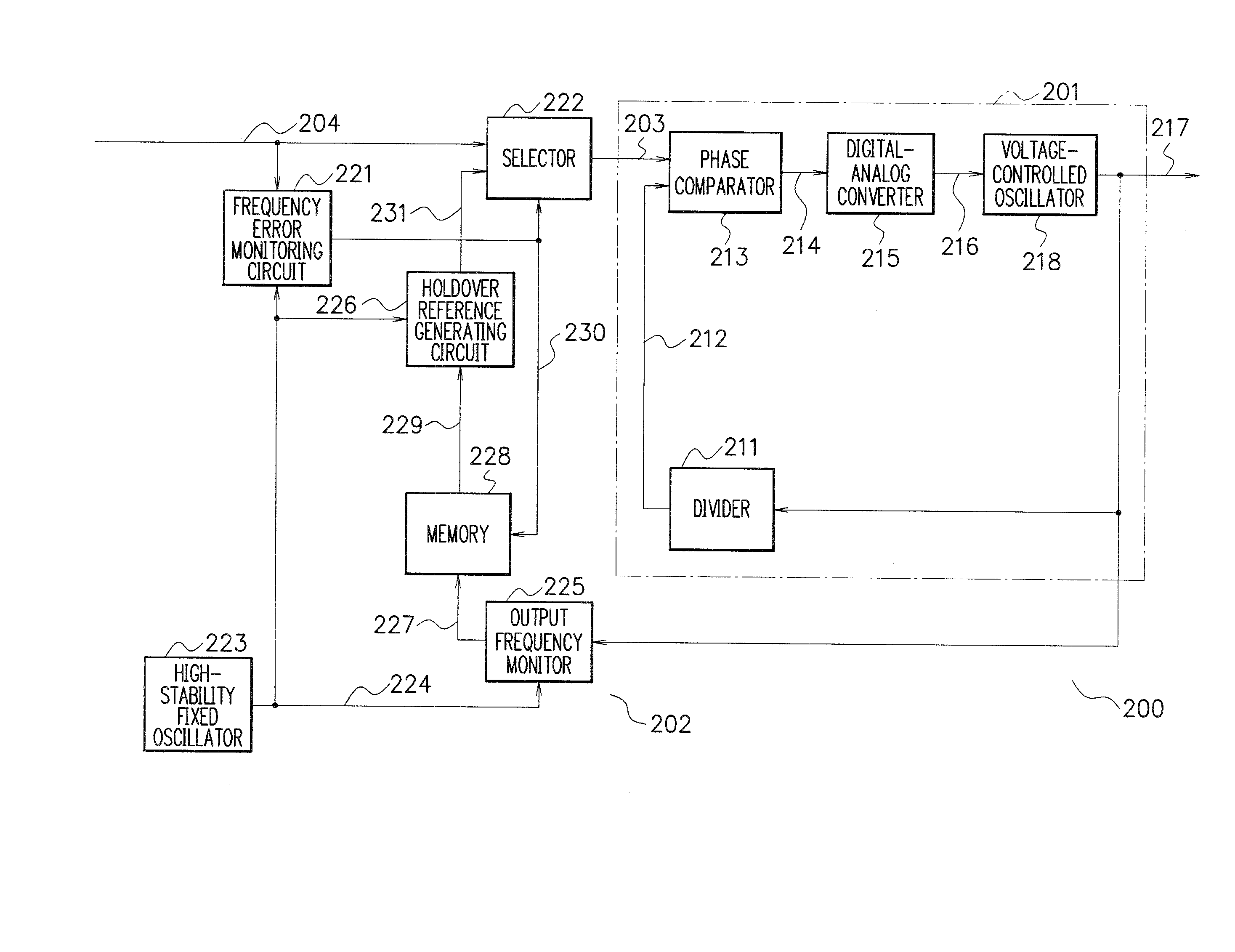
[0037]FIG. 1 schematically shows the structure of a clock supply device in accordance with one embodiment of the present invention. The clock supply device 200 has a holdover circuit unit 202 attached to a conventional PLL circuit 201 from the outside. The holdover circuit unit 202 has a holdover function. The PLL circuit 201 includes a phase comparator 213 that compares the phase of a signal 203 supplied from the holdover circuit unit 202 with the phase of an output 212 of a divider 211, a digital-analog converter 215 that receives a phase comparison result 214 and converts the result 214 into an analog signal, and a voltage-controlled oscillator 218 that receives an output 216 of the digital-analog converter 215 and outputs an output clock signal 217 having a frequency according to the output 216. The output clock signal 217 that is output from the voltage-controlled oscillator 218 serves as an output signal of the PLL circuit 201, and also branches into the divider 211. In the PL...
first modification
[First Modification]
[0110]FIG. 7 schematically shows the structure of a clock supply device in a first modification of the present invention. In the clock supply device 200A shown in FIG. 7, the same components as those of the clock supply device 200 of the embodiment shown in FIG. 1 are denoted by the same reference numerals as those shown in FIG. 1, and explanation of them is omitted here.
[0111] In the clock supply device 200A of the first modification, the output frequency monitor 225 shown in FIG. 1 does not exist, but an input frequency monitor 301 that monitors the frequency of the input reference signal 204 is provided instead. The input frequency monitor 301 receives the clock signal 224 output from the high-stability fixed oscillator 223 and the input reference signal 204, and stores a frequency monitor signal 302 as a digital signal representing the frequency of the input reference signal 204 in a memory 228A. Instead of the output frequency monitor value 229 of the embod...
second modification
[Second Modification]
[0117]FIG. 8 schematically shows the structure of a clock supply device in a second modification of the present invention. In the clock supply device 200B shown in FIG. 8, the same components as those of the clock supply devices 200 and 200A shown in FIG. 1 and FIG. 7 are denoted by the same reference numerals as those shown in FIG. 1 and FIG. 7, and explanation of them is omitted here.
[0118] The clock supply device 200B of the second modification has a circuit structure that combines the embodiment shown in FIG. 1 and the first modification shown in FIG. 7. More specifically, when an error occurs in the input reference signal 204 before synchronization of the PLL circuit 201 is completed, an input frequency monitor value 303A is read out from the memory 228A, and the input frequency monitor value 303A is supplied to a holdover reference generating circuit 226B via a selector 401 that is newly provided.
[0119] If an error is detected in the input reference sign...
PUM
 Abstract
Description
Claims
Application Information