NAND-type nonvolatile memory device and related method of manufacture

a nonvolatile, memory device technology, applied in the direction of semiconductor devices, basic electric elements, electrical equipment, etc., can solve the problems of insufficient exposure of underlying features, inconvenient manufacturing, and insufficient opening of openings, etc., to achieve the dimensions required for next-generation nand-type flash memory devices

Active Publication Date: 2008-04-03
SAMSUNG ELECTRONICS CO LTD
View PDF11 Cites 30 Cited by
  • Summary
  • Abstract
  • Description
  • Claims
  • Application Information

AI Technical Summary

Problems solved by technology

Unfortunately, if required processing conditions for a particular opening are not precisely met, the opening may not be properly formed.
For example, the opening may not adequately expose underlying features, or the opening may be formed wider than a desired width, creating possible electrical shorts.
Unfortunately, however, conventional manufacturing techniques are not well suited to forming openings with the dimensions required for next generation NAND type flash memory devices.

Method used


Image

  • NAND-type nonvolatile memory device and related method of manufacture
  • NAND-type nonvolatile memory device and related method of manufacture
  • NAND-type nonvolatile memory device and related method of manufacture

Examples


Embodiment Construction

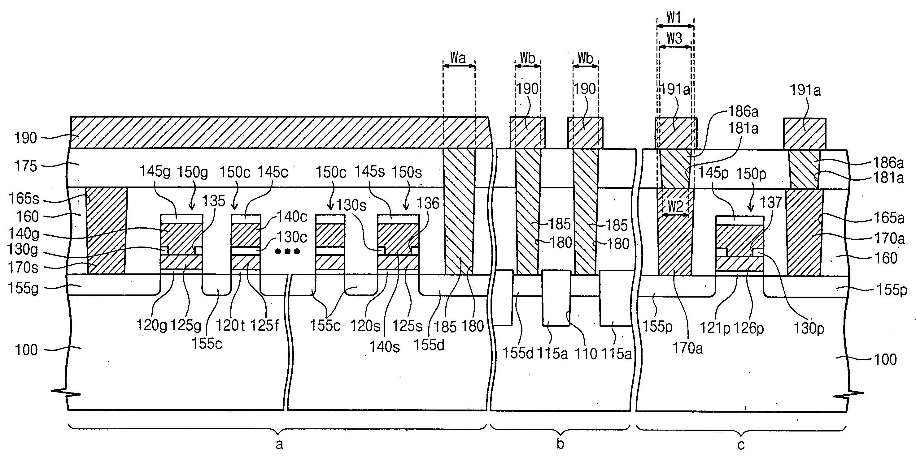
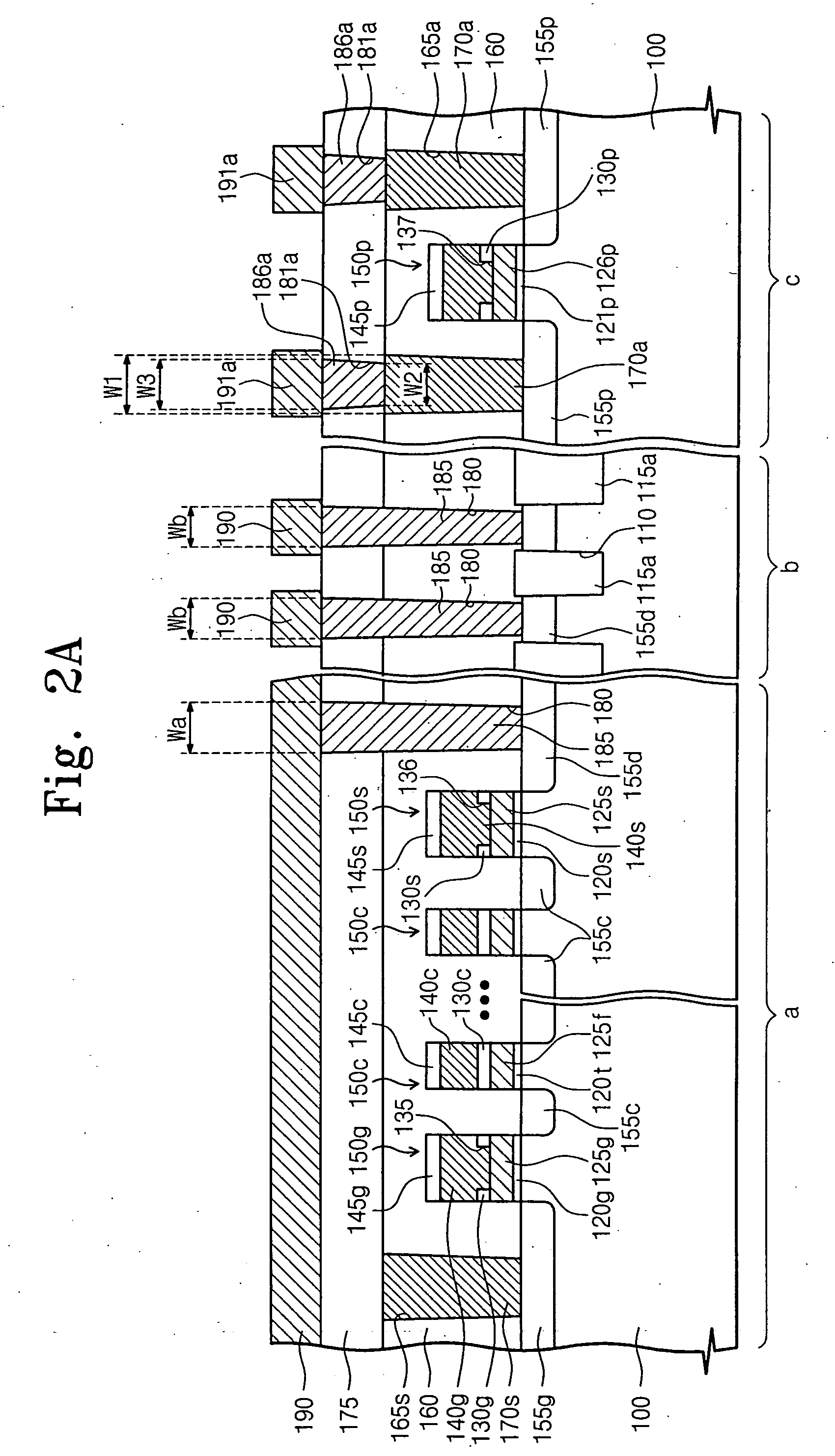
[0019]Exemplary embodiments of the invention are described below with reference to the corresponding drawings. These embodiments are presented as teaching examples. The actual scope of the invention is defined by the claims that follow.

[0020]In this written description, it should be understood that when one feature such as a layer or film is referred to as being “on” another feature such as another layer or a substrate, the one feature may be directly on the other feature, or intervening features may also be present. It should be further understood that when one feature such as a layer is referred to as being “under” another layer, the one feature can be directly under the other feature, or intervening features may be present. It should be still further understood that when one feature such as a layer is referred to as being “between” two other features, the one feature may be in direct contact with the other two features, or intervening features may be present.

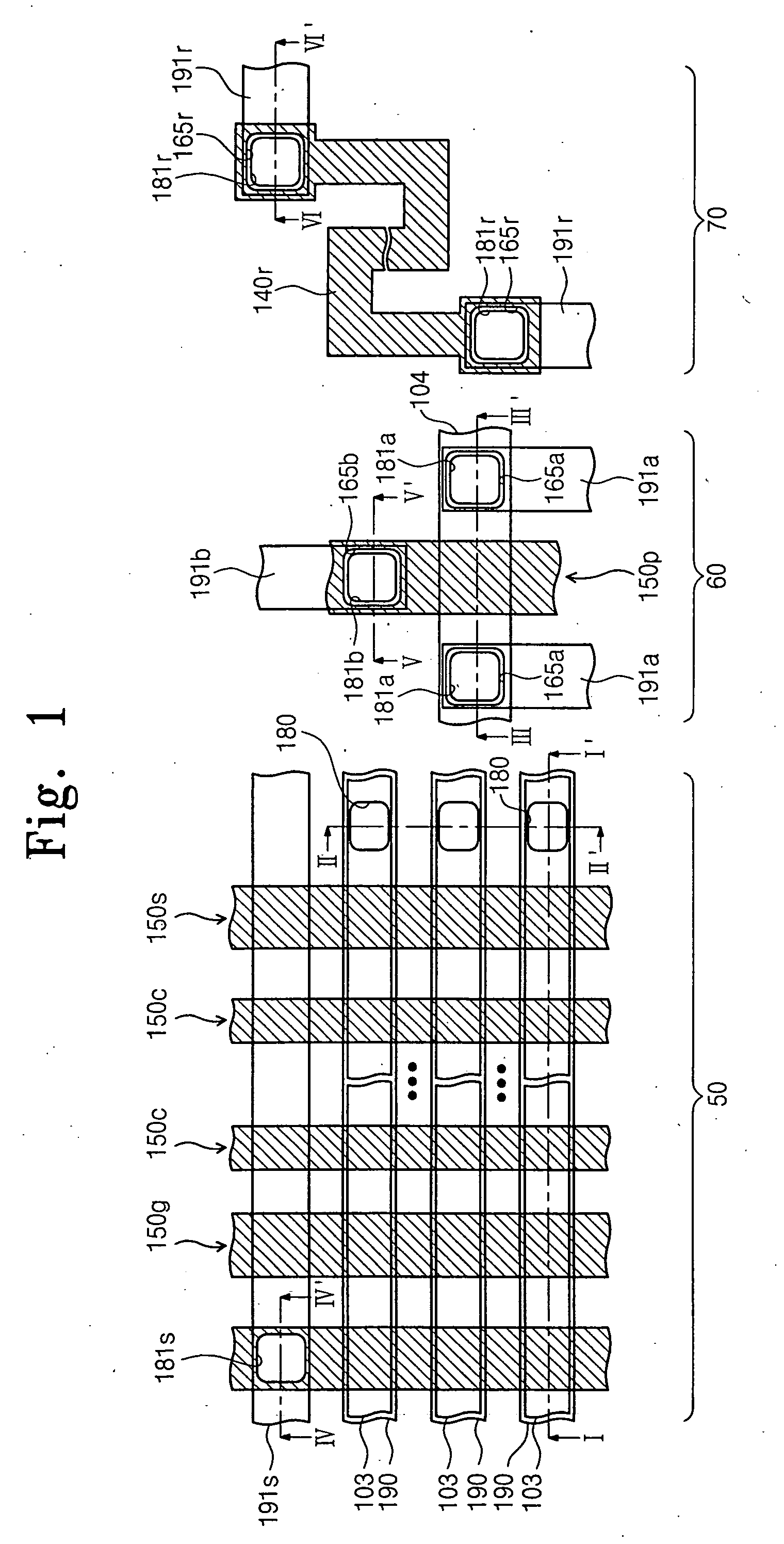
[0021]FIG. 1 is a pla...


PUM


Abstract

In a NAND type nonvolatile memory device, a first insulating layer covers a common drain region formed in a string active region and a peripheral active region. A second insulating layer covers the first insulating layer. A bit line plug penetrates the first and second insulating layers and is connected to the common drain region. A peripheral lower plug penetrates the first insulating layer and is connected to the peripheral active region. A peripheral upper plug penetrates the second insulating layer and is stacked on the peripheral lower plug.

Description

BACKGROUND OF THE INVENTION[0001]1. Field of the Invention[0002]Embodiments of the invention relate generally to semiconductor memory devices and related methods of manufacture. More particularly, embodiments of the invention relate to NAND-type nonvolatile semiconductor memory devices and related methods of manufacture.[0003]A claim of priority is made to Korean Patent Application No. 2006-97315 filed on Oct. 2, 2006, the disclosure of which is hereby incorporated by reference in its entirety.[0004]2. Description of Related Art[0005]Nonvolatile memory devices are capable of retaining stored data even when disconnected from an external power source. Among nonvolatile memory devices, flash memory is one of the more popular types due at least in part to its ability to be electrically programmed and erased, its relatively high degree of integration, resistance to physical stress, and low power consumption.[0006]Two common forms of flash memory include NOR-type flash memory and NAND typ...

Claims


Application Information

Patent Timeline
Patent Type & Authority Applications(United States)
IPC IPC(8): H01L29/76H01L21/82
CPCH01L27/115H01L27/11529H01L27/11526H10B41/40H10B41/41H10B69/00H01L29/40114H01L21/76897
Inventor PARK, HYUN-MOGLEE, SEUNG-JUNKIM, HYUN-JUNG
Owner SAMSUNG ELECTRONICS CO LTD
Why Eureka
Try Eureka