Test handler for testing semiconductor device and method of testing semiconductor device using the same

a technology of test handler and semiconductor device, which is applied in the direction of individual semiconductor device testing, semiconductor/solid-state device testing/measurement, instruments, etc., can solve the problems of difficult to maintain a high or low temperature in the test station chamber, and difficult to test the device in tim

Inactive Publication Date: 2008-04-03
SAMSUNG ELECTRONICS CO LTD
View PDF2 Cites 37 Cited by
  • Summary
  • Abstract
  • Description
  • Claims
  • Application Information

AI Technical Summary

Benefits of technology

[0009]Embodiments of the invention provide a test handler capable of assisting in efforts to maintain constant testing temperatures for test station chamber when a test head or a test board must be replaced or repaired, or even when a defect in the testing procedure is being addressed. Embodiments of the invention also provide a method of testing semiconductor devices using such a test handler.

Problems solved by technology

However, practical testing requires a significant throughput of tested devices.
Accordingly, it is difficult to properly maintain a high or low temperature within a test station chamber while changing out these elements.
Unfortunately, it is also very important to maintain a constant high or low temperature in the test station chamber when the test head (test board or test socket) is being repaired, replaced, or when a tester operating defect is being addressed.
This can take a great deal of time and slow testing throughput.

Method used


Image

  • Test handler for testing semiconductor device and method of testing semiconductor device using the same
  • Test handler for testing semiconductor device and method of testing semiconductor device using the same
  • Test handler for testing semiconductor device and method of testing semiconductor device using the same

Examples


Embodiment Construction

[0023]The present invention will now be described with reference to the accompanying drawings, in which exemplary embodiments of the invention are shown. The invention may, however, be embodied in many different forms and should not be construed as being limited to only the illustrated embodiments. Rather, the illustrated embodiments are provided so that this disclosure will be thorough and complete, and will fully convey the concept of the invention to those skilled in the art. In the drawings, the relative size of certain elements and regions may have been exaggerated for clarity of illustration.

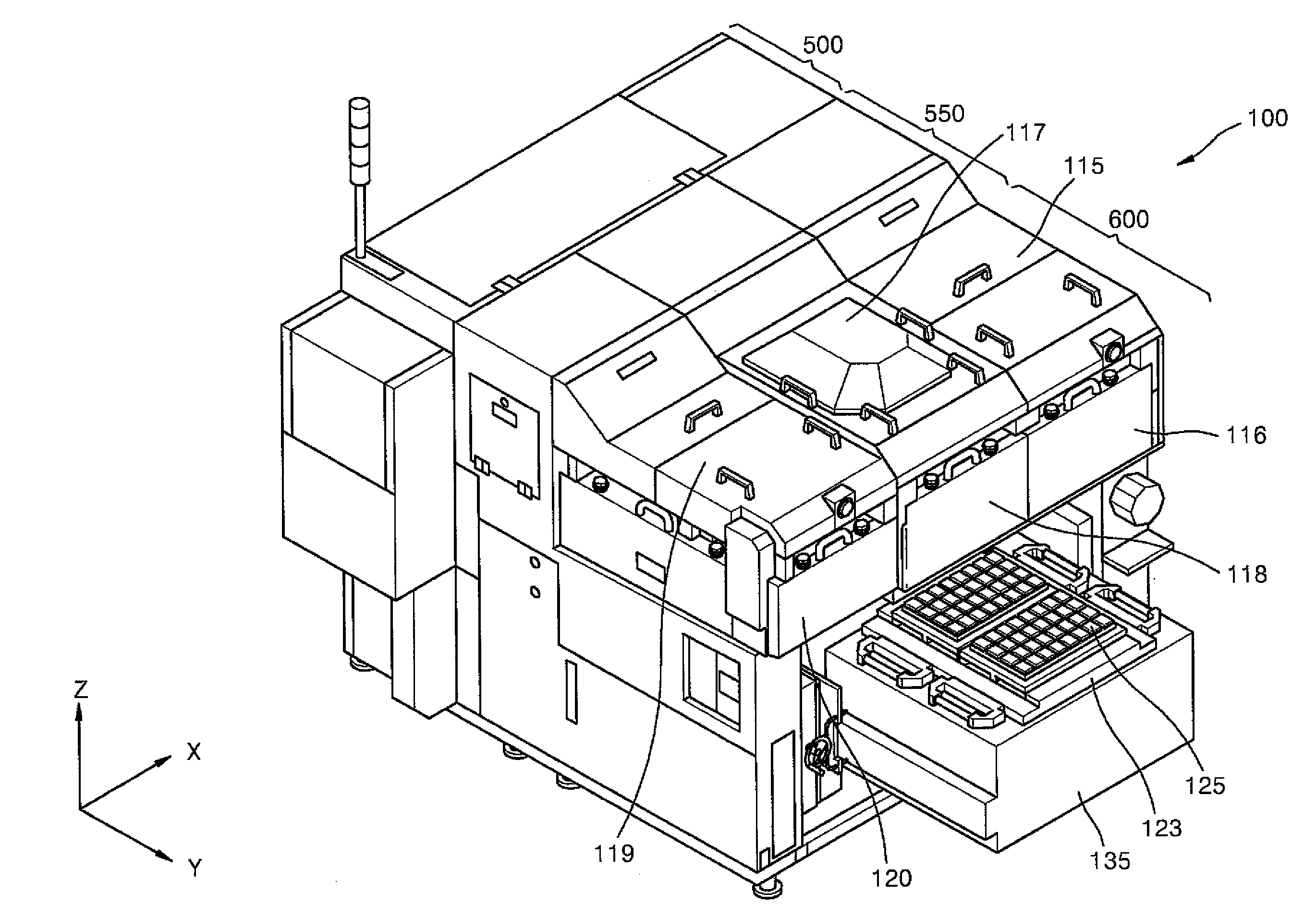
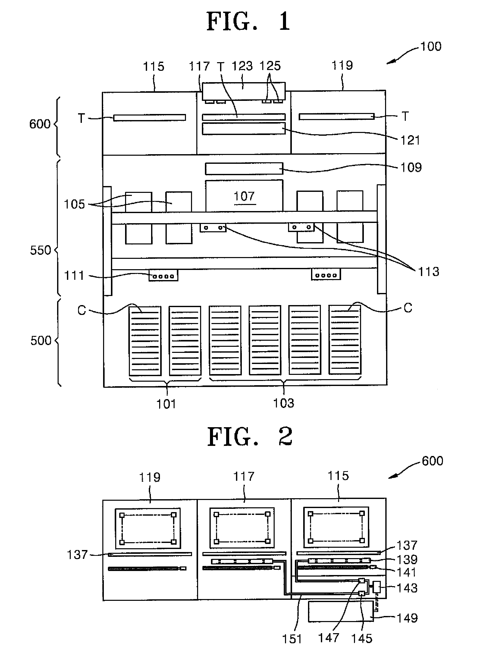
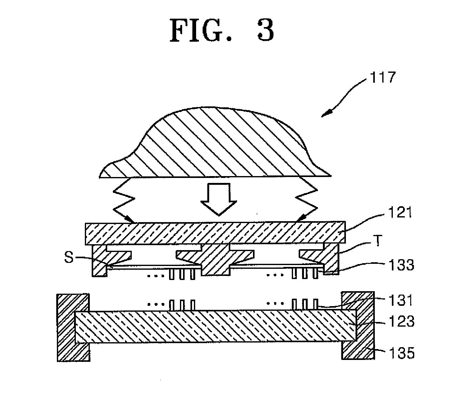
[0024]An exemplary configuration for a test handler according to an embodiment of the invention will be described briefly with reference to FIGS. 1 through 3. The test handler described in relation to FIGS. 1 through 3 can be a horizontal or lateral test handler. Throughout the written description and drawings, like reference numerals denote like or similar elements.

[0025]FIG. 1 is a schem...


PUM


Abstract

Provided is a test handler for testing a semiconductor device mounted in a test tray with a test head disposed separately below the test tray under predetermined testing condition at high or low temperature. The test handler includes a thermal isolator to maintain constant the predetermined testing condition at high or low temperature when the test chamber and the test head are separated. The thermal isolator is a shutter that is installed below the test chamber to seal or open the test chamber.

Description

CROSS-REFERENCE TO RELATED PATENT APPLICATION[0001]This application claims the benefit of Korean Patent Application No. 10-2006-0097406, filed on Oct. 2, 2006, the disclosure of which is hereby incorporated by reference.BACKGROUND OF THE INVENTION[0002]1. Field of the Invention[0003]The present invention relates to a test handler for testing semiconductor devices and a method of testing semiconductor devices using the test handler. More particularly, the invention relates to a test handler promoting maintenance of a constant temperature within a test chamber, and a method of testing semiconductor devices using the test handler.[0004]2. Description of Related Art[0005]In general, semiconductor devices, also referred to as integrated circuits (ICs), include memory devices, non-memory devices, and modules which mount a plurality of ICs on a wiring substrate. Following fabrication but before being shipped to customers or being incorporated within a host device, semiconductor devices mus...

Claims


Application Information

Patent Timeline
Patent Type & Authority Applications(United States)
IPC IPC(8): G01R31/26
CPCG01R31/2862G01R31/2893G01R31/2865G01R31/26H01L22/00
Inventor LEE, SUNG-SOO
Owner SAMSUNG ELECTRONICS CO LTD
Why Eureka
Try Eureka