Global predictive monitoring system for a manufacturing facility

a technology of global prediction and manufacturing facility, applied in the field of process monitoring system, can solve the problem of almost 80% of the yield loss in a fabrication facility

Active Publication Date: 2008-04-03
PDF SOLUTIONS SA
View PDF8 Cites 26 Cited by
  • Summary
  • Abstract
  • Description
  • Claims
  • Application Information

AI Technical Summary

Problems solved by technology

Moreover, because defectivity operations do not directly relate to device production, operators are inclined to bypass them.
These defects are responsible for almost 80% of the yield loss in a fabrication facility for a mature product.

Method used


Image

  • Global predictive monitoring system for a manufacturing facility
  • Global predictive monitoring system for a manufacturing facility
  • Global predictive monitoring system for a manufacturing facility

Examples


Embodiment Construction

Model of a Fabrication Facility

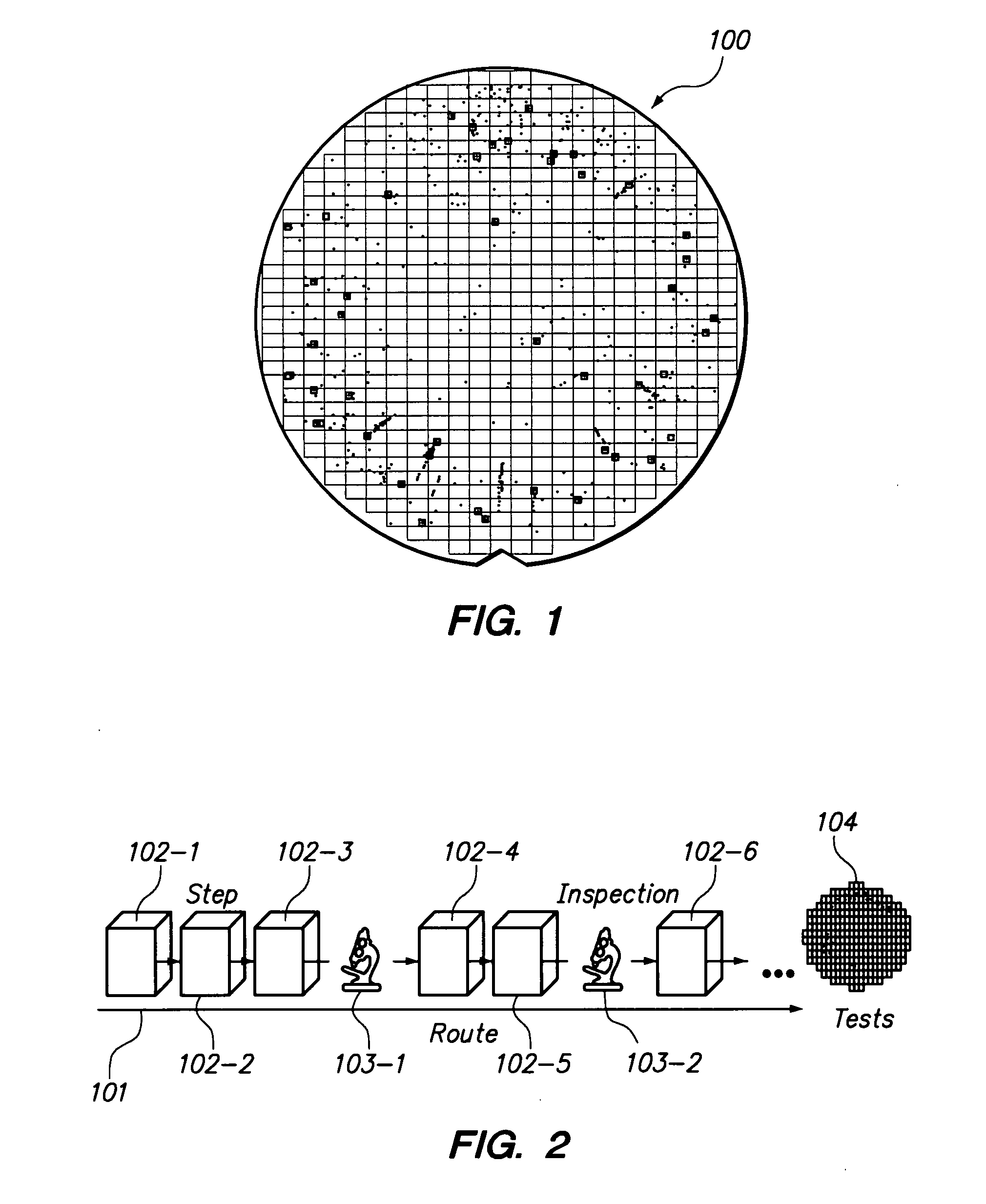
[0027]In some IC device fabrication facilities, defectivity operation steps are performed on particular wafer processing routes but can also be moved randomly to improve metrology sampling on specific parts of the production. FIG. 2 illustrates inspection steps dispatched over an example route of wafers in the fab. In the example of FIG. 2, a wafer processing route 101 includes production steps 102 (i.e., 102-1, 102-2, . . . ), inspection steps 103 (i.e., 103-1, 103-2, . . . ), and test steps 104. The production steps 102 may comprise steps for forming structures in wafers, such as deposition, lithorgraphy, etching, diffusion, annealing, implantation, polishing, etc. steps. The inspection steps 103 involve taking measurements of the wafers and may be performed between production steps 102. The test steps 104 involve testing of the wafers and may be performed at the end of production to compute the yield.

[0028]The processing route of the lot is largely ...


PUM


Abstract

A global predictive monitoring system for a manufacturing facility. The system may be employed in an integrated circuit (IC) device fabrication facility to monitor processing of semiconductor wafers. The system may include deployment of a swarm of individually separate agents running in computers in the facility. Each agent may comprise a genetic algorithm and use several neural networks for computation. Each agent may be configured to receive a limited set of inputs, such as defectivity data and WIP information, and calculate a risk from the inputs. A risk may be a value indicative of a production yield. Each agent may also generate a quality value indicative of a reliability of the risk value. New agents may be generated from the initial population of agents. Outputs from the agents may be collected and used to calculate projections indicative of a trend of the production yield.

Description

CROSS-REFERENCE TO RELATED APPLICATION[0001]This application claims the benefit of U.S. Provisional Application No. 60 / 846,562, filed on Sep. 22, 2006, entitled “Agent-Based Predictive Fab Monitoring System,” which is incorporated herein by reference in its entirety.BACKGROUND OF THE INVENTION[0002]1. Field of the Invention[0003]The present invention relates generally to process monitoring systems and more particularly, but not exclusively, to monitoring of integrated circuit device fabrication processes.[0004]2. Description of the Background Art[0005]A typical integrated circuit device fabrication facility or “fab” can process semiconductor wafers at a high rate to produce various devices. It is also not uncommon for processing of a single wafer to take almost three months and for different devices to be manufactured at the same time using the same equipments. Wafers may be grouped together in lots, with each lot being carried in a pod. All wafers in a pod are typically of the same...

Claims


Application Information

Patent Timeline
Patent Type & Authority Applications(United States)
IPC IPC(8): G06F19/00G06F15/16
CPCG05B23/0232G06N5/043G06N3/126
Inventor LACAILLE, JEROME HENRI NOEL
Owner PDF SOLUTIONS SA
Why Eureka
Try Eureka