Shear Force Sensing Device

a technology of sensing device and shear force, which is applied in the direction of force/torque/work measurement apparatus, instruments, manufacturing tools, etc., can solve the problems of increasing the frictional force and increasing the mechanical abrasion of materials, and achieves greater frictional force, mechanical abrasion, and increased frictional force

Active Publication Date: 2008-04-17
KLA TENCOR TECH CORP
View PDF17 Cites 21 Cited by
  • Summary
  • Abstract
  • Description
  • Claims
  • Application Information

AI Technical Summary

Benefits of technology

[0007] In general, removal of material in CMP is caused by two mechanisms: mechanical action and chemical action. Although these mechanisms are closely linked, it may be desirable to try to separately measure parameters associated with each. One measurement that may be of particular value in measuring mechanical action is the frictional force between a wafer and a pad as the wafer moves with respect to the pad. Generally, mechanical abrasion of material increases with increasing frictional force. Frictional force may be used to provide a shear force in a structure that deforms in a manner that indicates the magnitude of the shear force. In general, greater frictional force provides greater mechanical action in removing material during CMP.

Problems solved by technology

Generally, mechanical abrasion of material increases with increasing frictional force.

Method used


Image

  • Shear Force Sensing Device
  • Shear Force Sensing Device
  • Shear Force Sensing Device

Examples


Embodiment Construction

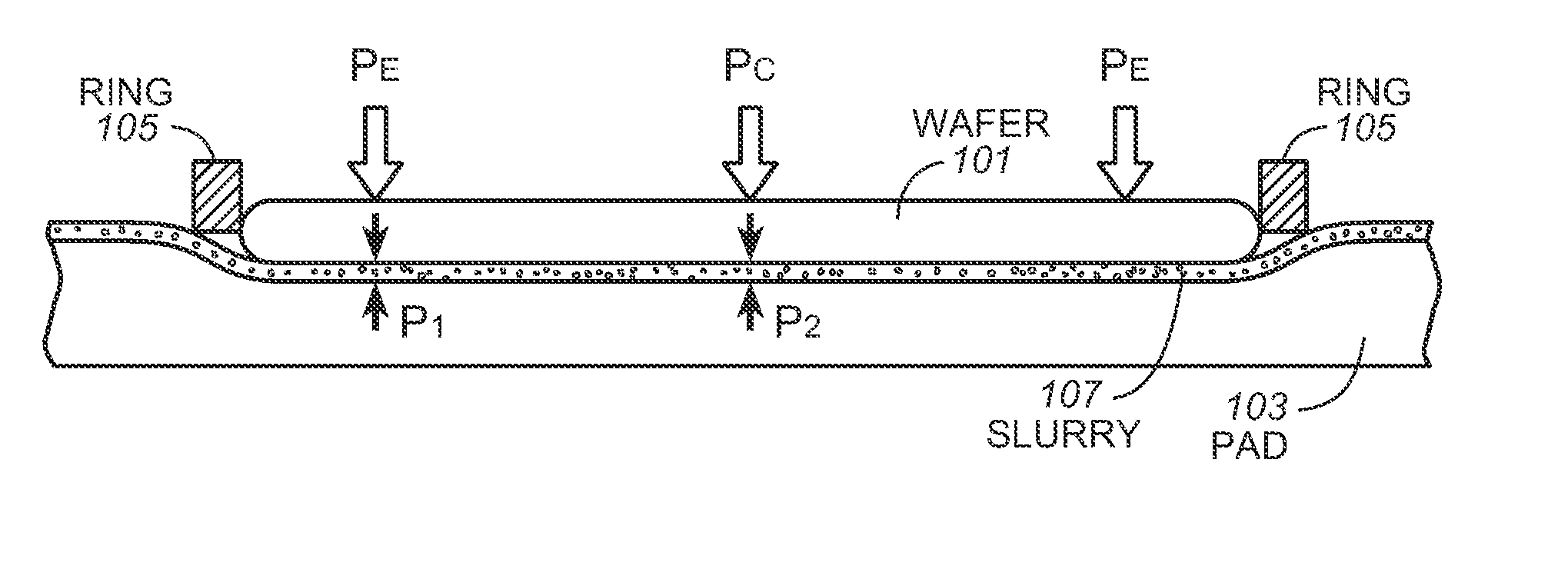
[0040] Process Condition Measuring Devices (PCMDs) include instrumented wafers that have physical dimensions the same, or close to, those of a production wafer and that include sensors and electronics to measure at least one process condition. Various PCMDs are described in U.S. patent application Ser. Nos. 10 / 718,269, 10 / 837,359 and 11 / 381,992. PCMDs may be wired or wireless. A wired PCMD sends data to an external unit over wires (or optical fibers). A wireless PCMD either stores data in a memory in the PCMD or may transmit the data to an external unit. Generally, wireless PCMDs are more suitable for studying processes where a wafer is rotated such as CMP.

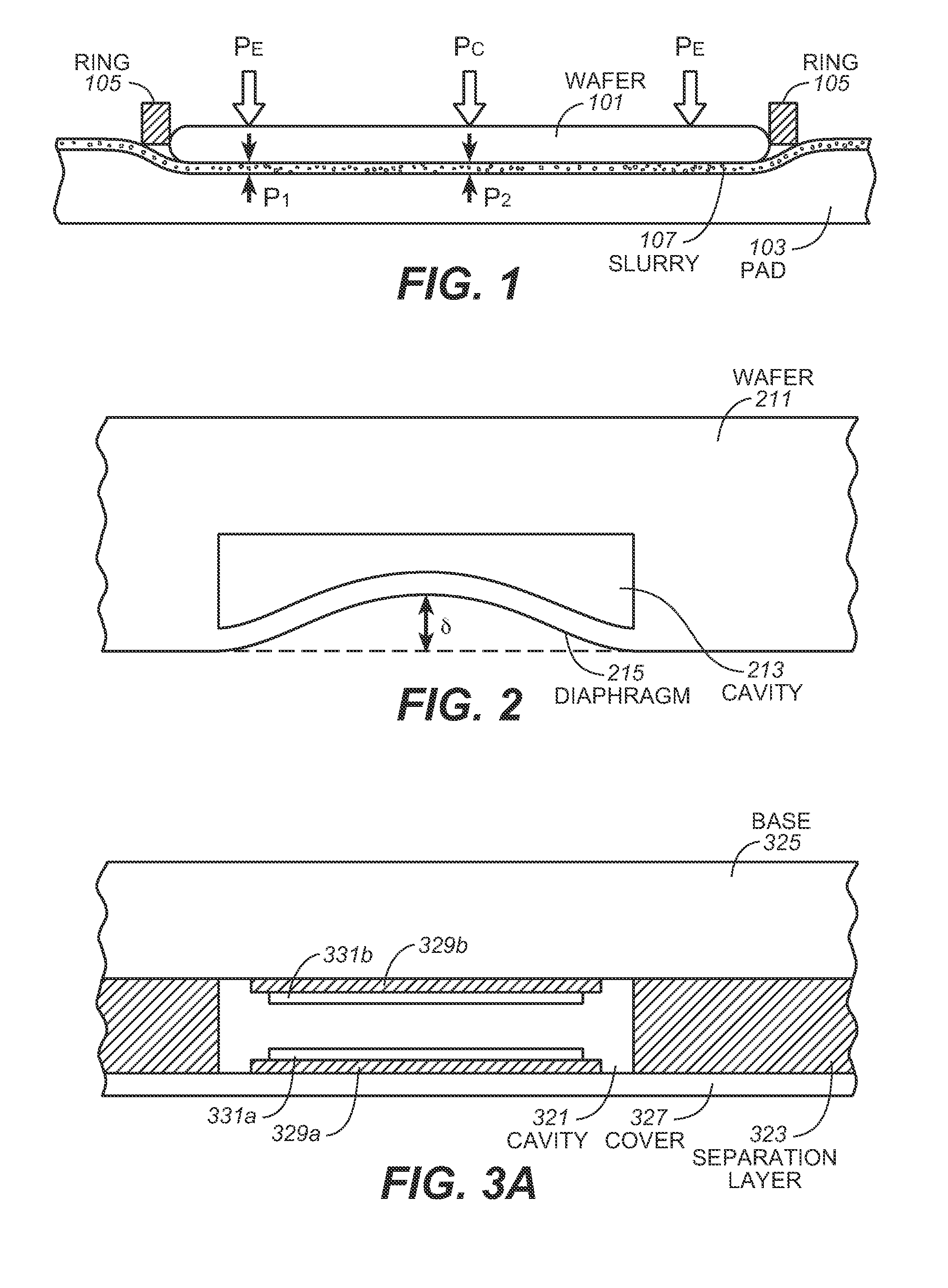
[0041] One way to measure pressure on a wafer surface is to form a cavity within the wafer, leaving a thin layer over the cavity that acts as a diaphragm and deflects under pressure. FIG. 2 shows an example of a wafer 211 having a cavity 213 that is covered by a diaphragm 215. Under pressure, the diaphragm 215 deflects by an amou...


PUM

PropertyMeasurementUnit
Pressureaaaaaaaaaa
pressuresaaaaaaaaaa
thickaaaaaaaaaa

Abstract

At least one shear force sensor is used to measure the shear force on a member, when the member is in contact with and pressed against a polishing or planarization surface and a lateral force is applied between the two surfaces. Preferably the structure and the surface of the structure have properties (such as one or more of the following: dimensions and coefficient of friction) that are substantially the same as those of a real substrate, such as a semiconductor wafer or flat panel display panel.

Description

CROSS-REFERENCE TO RELATED APPLICATION [0001] This non-provisional application claims the benefit of provisional applications No. 60 / 828,000, filed Oct. 3, 2006, by Wayne G. Renken et al., entitled “Pressure Sensing Wafer,” and No. 60 / 828,351, filed Oct. 5, 2006, by Wayne G. Renken et al., entitled “Pressure Sensing Wafer,” which applications are incorporated herein in their entireties by this reference. This application is also related to an application Ser. No. 11 / 392,220, filed Mar. 28, 2006, by Randall S. Mundt, entitled “Apparatus for Measurement of Paramenters in Process Equipment,” also incorporated herein in its entirety by this reference. This application is also related to an application filed on the same day as this application, entitled “Pressure Sensing Device,” by Wayne G. Renken et al., also incorporated herein in its entirety by this reference.BACKGROUND OF THE INVENTION [0002] Semiconductor processing involves multiple steps to produce working integrated circuits on...

Claims


Application Information

Patent Timeline
Patent Type & Authority Applications(United States)
IPC IPC(8): G01L1/20G01N27/04
CPCG01L1/148G01L9/0073G01L9/0042G01L5/0047
Inventor RENKEN, WAYNE G.SUN, MEI H.MASON, ARON ABRAMOWSKI
Owner KLA TENCOR TECH CORP
Why Eureka
Try Eureka