

Solid-state imaging apparatus
a technology of solid-state imaging and imaging apparatus, which is applied in the direction of color television details, television systems, radioation control devices, etc., can solve problems such as image distortion
- Summary
- Abstract
- Description
- Claims
- Application Information
AI Technical Summary
Benefits of technology
Problems solved by technology
Method used
Image

Examples
embodiment 1
[0028]A fundamental construction of electronic camera using the solid-state imaging apparatus according to a first embodiment of the invention will now be described by way of the block diagram in FIG. 5. FIG. 5 includes: 11, an imaging optical system; 12, a solid-state imaging device; 13, A / D converter; 14, a signal processing circuit containing an interpolation processing circuit; 15, a memory; 16, a recording apparatus; 17, an optical system control circuit; 18, a drive circuit of the solid-state imaging device 12; and 19, a control apparatus for controlling each section.
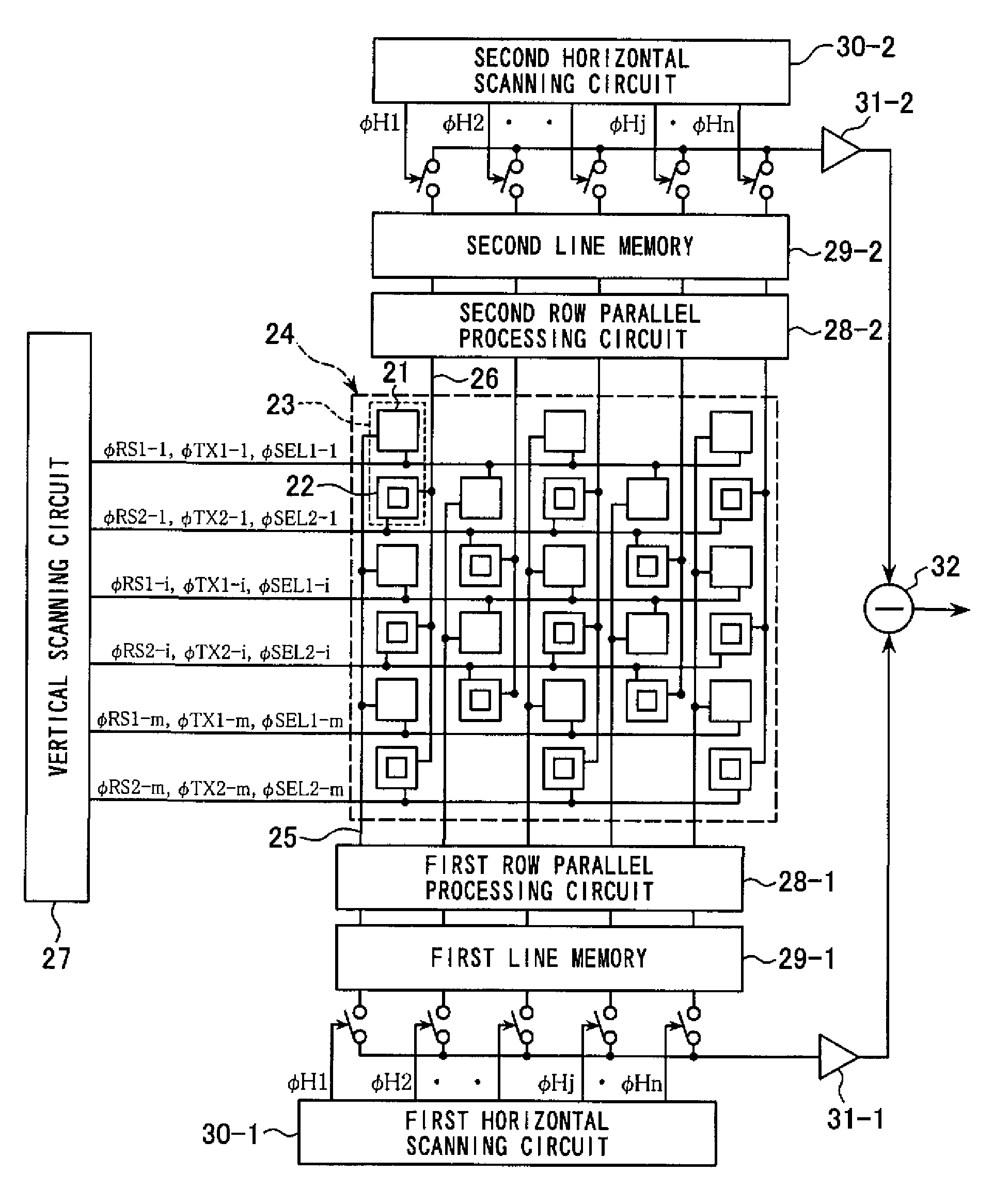
[0029]A construction of the solid-state imaging device in the solid-state imaging apparatus according to the first embodiment of the invention will now be described by way of a block diagram shown in FIG. 6. Referring to FIG. 6, numeral 21 denotes a first pixel and 22 denotes a second pixel, the first pixel and adjacent second pixel forming a unit pixel 23. Of a plurality of unit pixel columns arranged in the vert...
embodiment 2
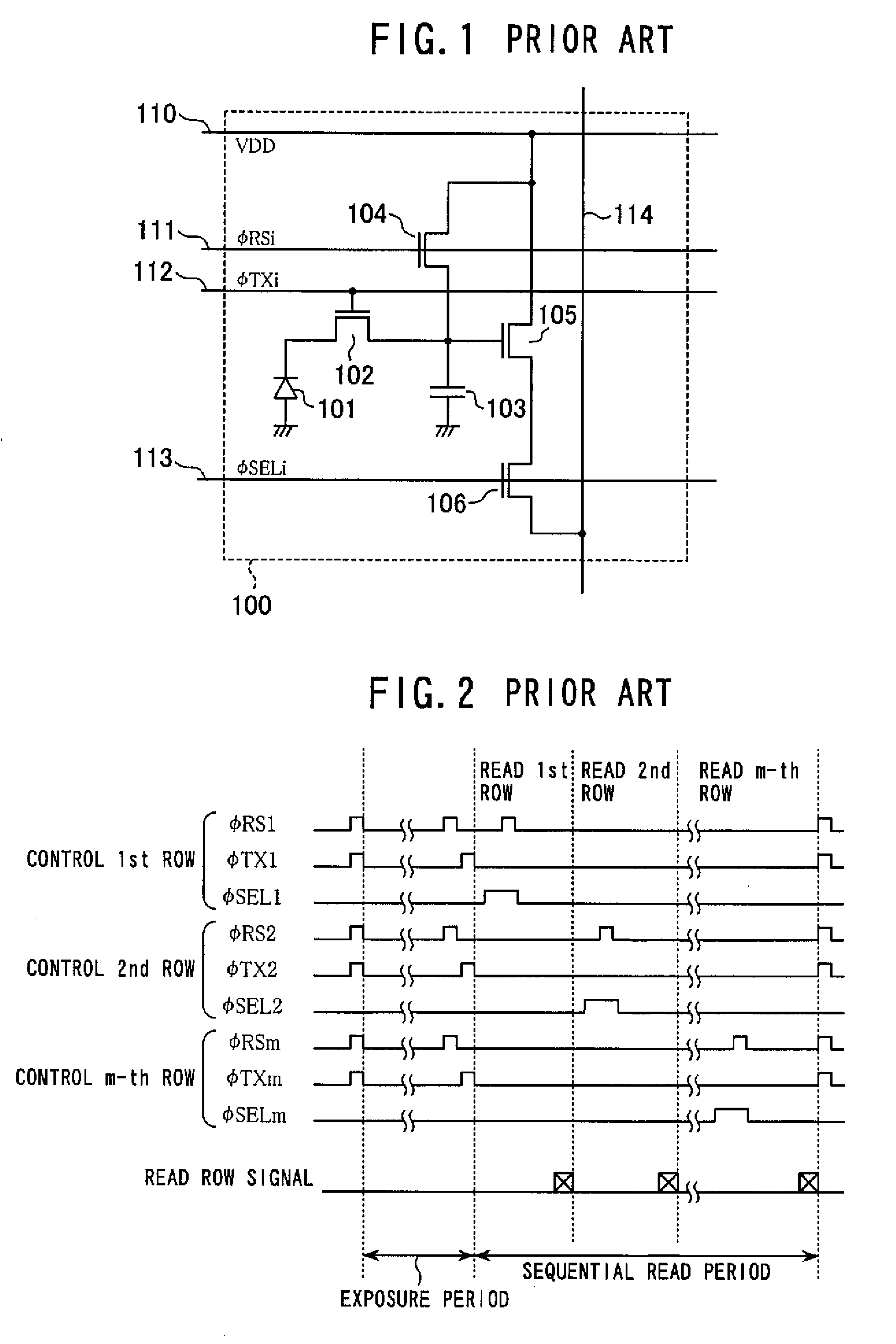
[0039]The solid-state imaging apparatus according to a second embodiment of the invention will now be described. A general construction of the solid-state imaging device and construction of the unit pixel according to the second embodiment are similar to the first embodiment, and only difference is the drive method of the pixel section 24 by the drive circuit 18. An explanation based on a diagrammatic representation of the solid-state imaging device will thus be omitted, and the drive method of the solid-state imaging device according to the second embodiment will be described by way of the timing chart shown in FIG. 10. First, the first reset signal φRS1-1 to φRS1-m and first transfer signal φTX1-1 to φTX1-m are inputted to the first pixel 21 of the unit pixels 23 of all rows of the pixel section 24 to concurrently reset the photodiode and charge accumulation section of the first pixel 21 of the unit pixels of all rows. Next, after passage of a predetermined time (exposure time), t...
PUM
 Abstract
Description
Claims
Application Information