Modulation circuit having DC offset level control circuit

a level control circuit and module technology, applied in the field of modules, can solve the problems of increasing the size of the circuit, affecting the signal quality, and difficult to cancel the carrier leakage with high accuracy, so as to suppress the carrier leakage and suppress the increase of the circuit size

Inactive Publication Date: 2008-04-17
RENESAS ELECTRONICS CORP
View PDF3 Cites 10 Cited by
  • Summary
  • Abstract
  • Description
  • Claims
  • Application Information

AI Technical Summary

Benefits of technology

[0011]According to the modulation circuit of the present invention, it is possible to suppress the carrier leak by correcting a DC offset component and to control the gain at the same time. Also it is possible to suppress an increase of a size of the circuit.
[0012]According to the modulation circuit of the present invention, it is possible to suppress the carrier leak and to control the gain at the same time.

Problems solved by technology

When the DC offset occurs, a carrier frequency component called carrier leak appears in an output frequency, which causes a degradation of a signal quality.
However, in the technology disclosed in Japanese Unexamined Patent Application Publication No. 2005-295376, there is a need to demodulate the signal modulated by the orthogonal modulator 82 by the carrier leak regulator 83 again, which increases a size of the circuit.
In the technology disclosed in Japanese Patent No. 3308811, there is a need to create a signal which has the opposite phase to the carrier leak and which has the same amplitude to the carrier leak by a cancel carrier wave signal, which makes it difficult to cancel the carrier leak with high accuracy.
In the technologies disclosed in Japanese Unexamined Patent Application Publication No. 2005-295376 and Japanese Patent No. 3308811, it is difficult to control the gain and suppress the carrier leak while suppressing the size of the circuit.
As stated above, in the conventional modulation circuits, it is difficult to suppress the carrier leak and control the gain while suppressing the size of the circuit.

Method used


Image

  • Modulation circuit having DC offset level control circuit
  • Modulation circuit having DC offset level control circuit
  • Modulation circuit having DC offset level control circuit

Examples


embodiment 1

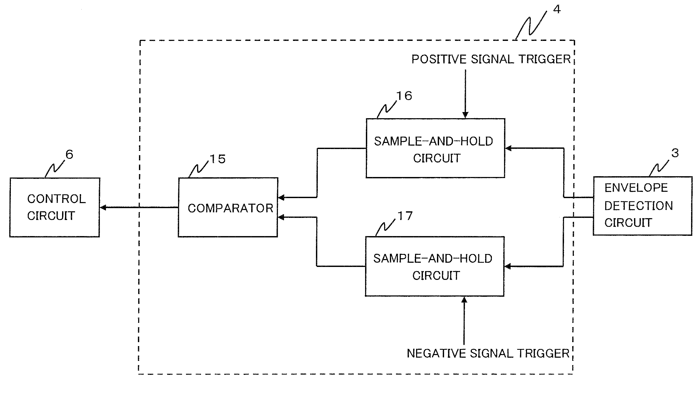
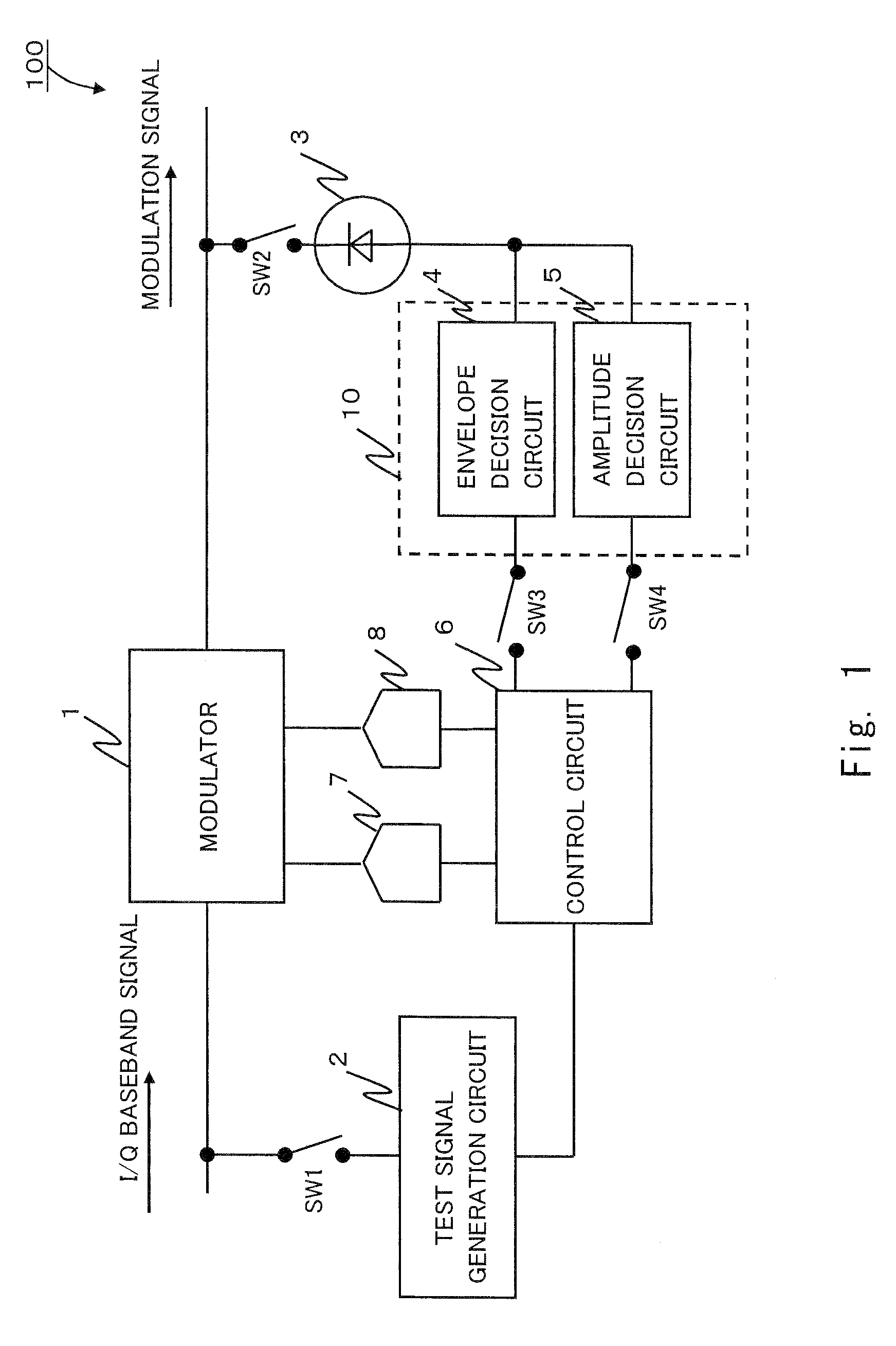
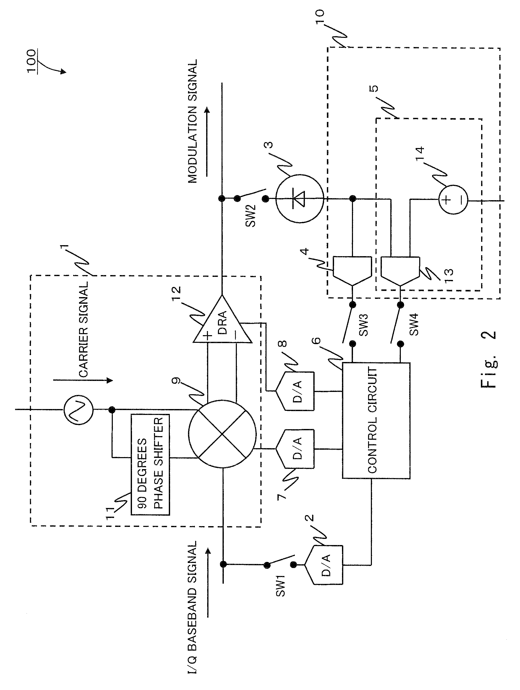
[0023]The embodiment of the present invention will now be described with reference to the drawings. FIG. 1 is a block diagram showing a typical modulation circuit according to the embodiment 1 of the present invention. As shown in FIG. 1, the modulation circuit 100 of this embodiment includes a modulator 1, a test signal generation circuit 2, a detector (hereinafter referred to as envelope detection circuit) 3, a first controller, and a second controller. The first controller includes a decision circuit 10, a control circuit 6, and a first control circuit (hereinafter referred to as DC offset regulation circuit) 7. The second controller includes the decision circuit 10, the control circuit 6, and a second control circuit (hereinafter referred to as gain regulation circuit) 8. The decision circuit 10 includes an envelope decision circuit 4 and an amplitude decision circuit 5. FIG. 2 is a block diagram showing a typical modulation circuit shown in FIG. 1 more specifically. The modulat...


PUM


Abstract

A modulation circuit according to the present invention includes: a modulator modulating a received signal and outputting a modulated signal; a detector circuit receiving the modulated signal and outputting a envelope of the modulated signal; and a first controller regulating an offset level of the modulator based on the envelope.

Description

BACKGROUND OF THE INVENTION[0001]1. Field of the invention[0002]The present invention relates to a modulation circuit, and more specifically to a modulation circuit that includes a DC offset level control circuit.[0003]2. Description of Related Art[0004]A modulation circuit has conventionally been used for communication systems. The modulation circuit is a circuit outputting a modulation signal based on a baseband signal and a carrier wave (hereinafter referred to as carrier). When the modulation circuit is used, a DC offset can occur in the modulation circuit due to a disturbance of an element, for example. To be more precise, for example, the DC offset occurs in I / Q base band signals inputted to a orthogonal modulator when a orthogonal modulation is performed using the orthogonal modulator. When the DC offset occurs, a carrier frequency component called carrier leak appears in an output frequency, which causes a degradation of a signal quality. Japanese Unexamined Patent Applicati...

Claims


Application Information

Patent Timeline
Patent Type & Authority Applications(United States)
IPC IPC(8): H04L27/14
CPCH04L27/364H04L25/061H03C1/06H04L2027/0016
Inventor KOMATSU, YASUSHI
Owner RENESAS ELECTRONICS CORP
Why Eureka
Try Eureka