Optical control device

Active Publication Date: 2013-09-19
SUMITOMO OSAKA CEMENT CO LTD
View PDF5 Cites 10 Cited by
  • Summary
  • Abstract
  • Description
  • Claims
  • Application Information

AI Technical Summary

Benefits of technology

[0014]According to the first aspect of the present invention, since the modulation electrode includes at least two signal electrodes and ground electrodes disposed to interpose the signal electrodes therebetween and the electrical connection member disposed to cross over part of the signal electrode is used to electrically connect the ground electrode disposed between the two signal electrodes to other ground electrodes, it is possible to reinforce and stabilize the ground state of the ground electrodes and to prevent an electric field formed by the signal electrodes from going over the ground electrodes and affecting the neighboring signal electrodes or optical waveguides. Since the ground state of the ground electrodes is reinforced and stabilized by the electrical connection member, it is not necessary to increase the gap between the optical waveguides or the gap between the signal electrodes, unlike the related art, and it is thus possible to suppress an increase in size of the optical control device.
[0015]According to the second aspect of the present invention, since the electrical connection member is disposed in the interaction portion in which the modulation electrode modulates the optical waves, it is possible to suppress degradation of signal light in the interaction portion which is most important in forming signal light and it is thus possible to provide an optical control device with excellent optical characteristics such as an extinction ratio of signal light.
[0016]According to the third aspect of the present invention, since the modu

Problems solved by technology

In order to suppress the crosstalk between electrodes, it is effective to increase the gap between the optical waveguides or the gap between the electrodes, but this method causes an increase in device size, which is not desirable.
However, since a process of forming the groove is particularly added to the optical control device manufacturing process, the manufacturing time and cost increase.
In optica

Method used


Image

  • Optical control device
  • Optical control device
  • Optical control device

Examples


Embodiment Construction

Description of Embodiments

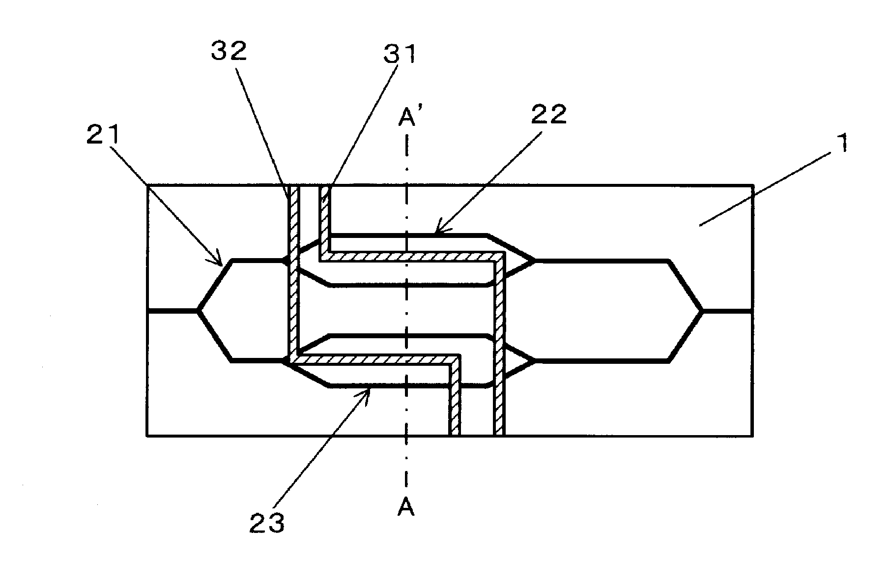
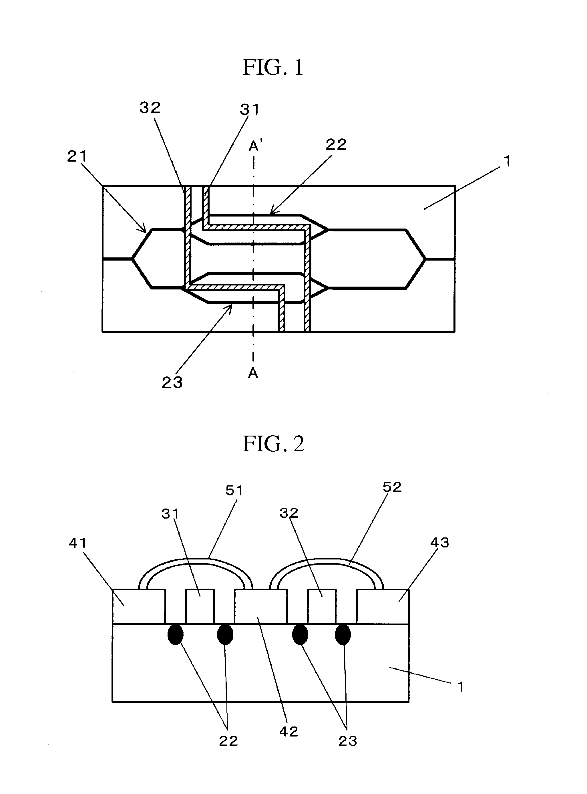
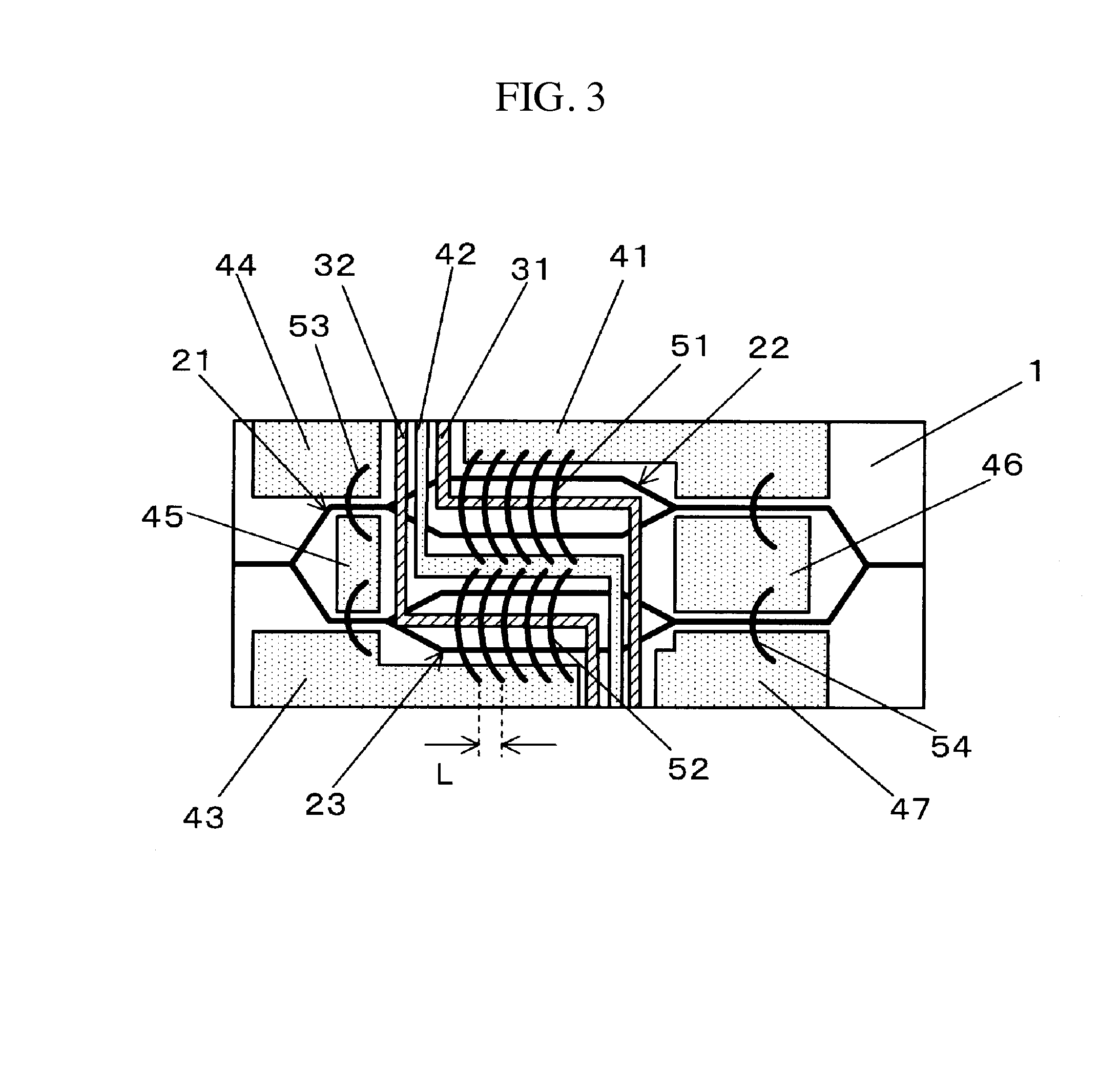
[0022]Hereinafter, an optical control device according to the present invention will be described in detail with reference to a suitable example. FIG. 1 is a diagram schematically illustrating the configuration of an optical control device according to the present invention and FIG. 2 is a cross-sectional view taken along one-dotted chain line A-A′ of FIG. 1. As shown in FIGS. 1 and 2, the optical control device according to the present invention includes a substrate 1 having an electro-optical effect, optical waveguides 21 to 23 formed in the substrate, and a modulation electrode modulating optical waves propagating in the optical waveguides, the modulation electrode includes at least two signal electrodes 31 and 32 and ground electrodes 41 to 43 arranged to interpose the signal electrodes therebetween, and the optical control device further includes electrical connection members 51 and 52 that electrically connects the ground electrode disposed between th...


PUM


Abstract

An optical control device is provided which can suppress crosstalk between electrodes without increasing the entire size of the device itself. The optical control device includes a substrate having an electro-optical effect, an optical waveguide formed in the substrate, and a modulation electrode modulating optical waves propagating in the optical waveguide. The modulation electrode includes at least two signal electrodes and ground electrodes arranged to interpose the signal electrodes therebetween. The optical control device further includes an electrical connection member that electrically connects the ground electrode disposed between the two signal electrodes to other ground electrodes and that is disposed to cross over part of the signal electrode.

Description

BACKGROUND OF THE INVENTION[0001]1. Field of the Invention[0002]The present invention relates to an optical control device, and more particularly, to an optical control device having two or more signal electrodes as a modulation electrode.[0003]2. Description of Related Art[0004]Optical control devices have been used in which optical waveguides and modulation electrodes are formed in a substrate such as lithium niobate or the like having an electro-optical effect and optical waves propagating in the optical waveguides are modulated by the modulation electrodes. Recently, in order to meet requirements such as an increase in communication speed or an increase in communication data rate in the fields of optical communications or the like, plural Mach-Zehnder type optical waveguides (MZ-type optical waveguides) are driven using plural modulation signals in a differential quadrature phase shift keying (DQPSK) format.[0005]In an optical control device having plural optical waveguides and ...

Claims


Application Information

Patent Timeline
IPC IPC(8): G02F1/035
CPCG02F1/035G02F2201/121G02F1/0356
Inventor KANNO, SHINSUKESHIMIZU, RYO
Owner SUMITOMO OSAKA CEMENT CO LTD
Why Eureka
Try Eureka