

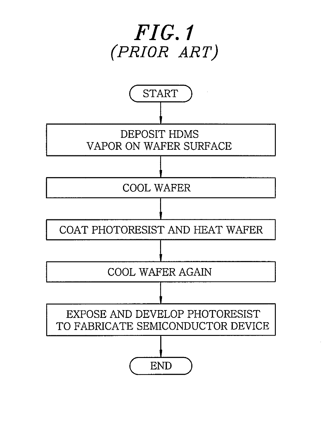
Method of fabricating semiconductor device
a semiconductor and device technology, applied in the field of semiconductor device manufacturing, can solve the problems of high material cost and manufacturing delays, inability to achieve adequate adhesion, and frequent removal of defective photoresist patterns, so as to reduce the increase in processing time and material waste, and improve productivity.
- Summary
- Abstract
- Description
- Claims
- Application Information
AI Technical Summary
Benefits of technology
Problems solved by technology
Method used
Image

Examples
Embodiment Construction
[0007] In general, example embodiments of the invention relate to a method of fabricating a semiconductor device capable of saving manufacturing time and improving productivity by suppressing an increase in the processing time and a waste of materials caused by defective photoresist patterns.
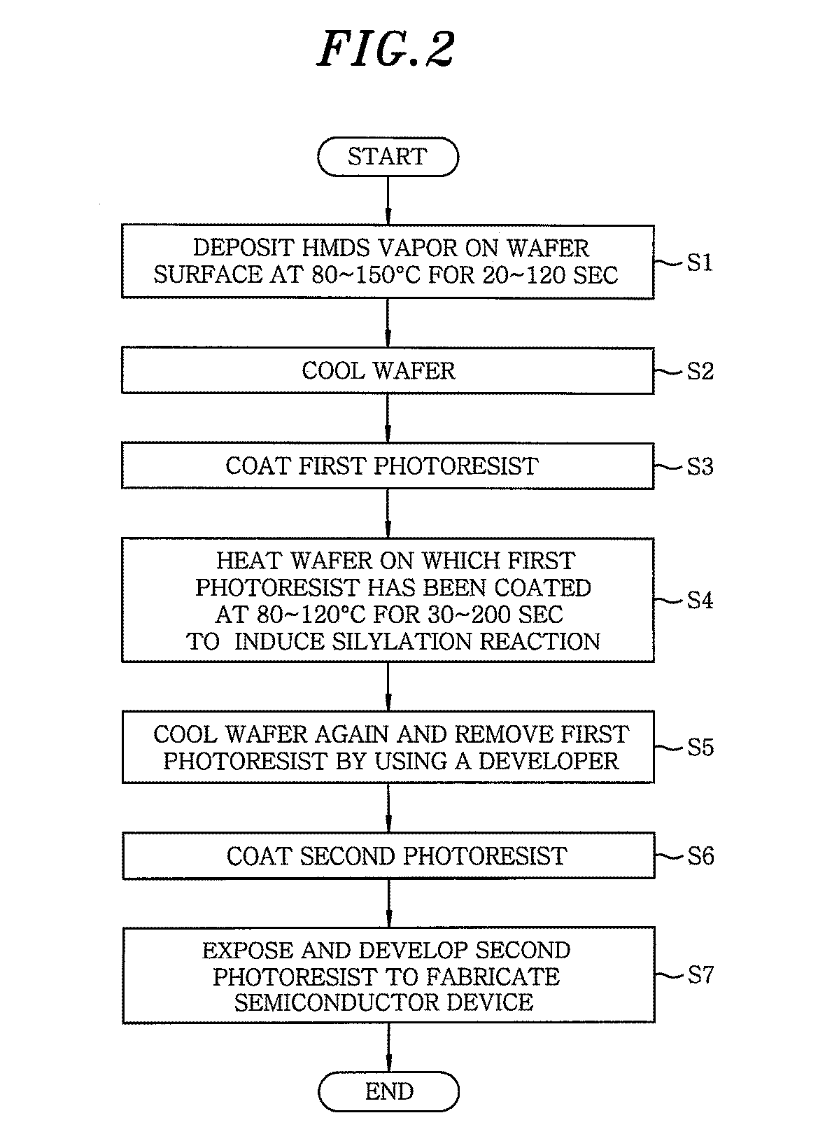
[0008] In accordance with an example embodiment, there is provided a method of fabricating a semiconductor device, including the steps of depositing HMDS on a wafer surface, cooling the wafer and coating the wafer surface with a first photoresist, heating the wafer on which the first photoresist has been coated to induce a silylation reaction, cooling the wafer, and developing and removing the first photoresist.
[0009] The HMDS can be deposited on the wafer in a temperature range of 80 to 150 degrees Celsius for 20 to 120 seconds.
[0010] The first photoresist can include a negative-based photoresist or a thermosetting photoresist.
[0011] The first photoresist can be heated in a temperature rang...
PUM
| Property | Measurement | Unit |
|---|---|---|
| temperature | aaaaa | aaaaa |
| temperature | aaaaa | aaaaa |
| temperature | aaaaa | aaaaa |
Abstract
Description
Claims
Application Information