Method and Apparatus for Non-Volatile Multi-Bit Memory

a multi-bit memory and non-volatile technology, applied in the direction of digital storage, semiconductor devices, instruments, etc., can solve the problems of affecting the development of the industry, and affecting the development of the next generation of devices

Active Publication Date: 2008-04-24
MACRONIX INT CO LTD
View PDF8 Cites 53 Cited by
  • Summary
  • Abstract
  • Description
  • Claims
  • Application Information

AI Technical Summary

Problems solved by technology

Problems have arisen in manufacturing such devices with very small dimensions, and with variations in process that meets tight specifications needed for large-scale memory devices.
Moreover, as increases in capacity have led to decreases in the sizes required for such devices, the industry is approaching the area where physical limits, imposed, for example, by the size of the atoms involved, are impeding future developments.

Method used


Image

  • Method and Apparatus for Non-Volatile Multi-Bit Memory
  • Method and Apparatus for Non-Volatile Multi-Bit Memory
  • Method and Apparatus for Non-Volatile Multi-Bit Memory

Examples


Embodiment Construction

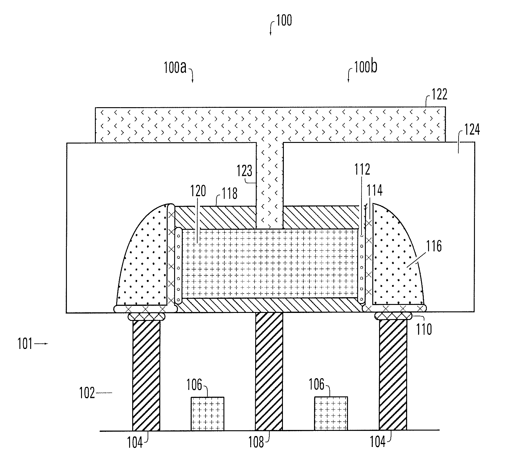
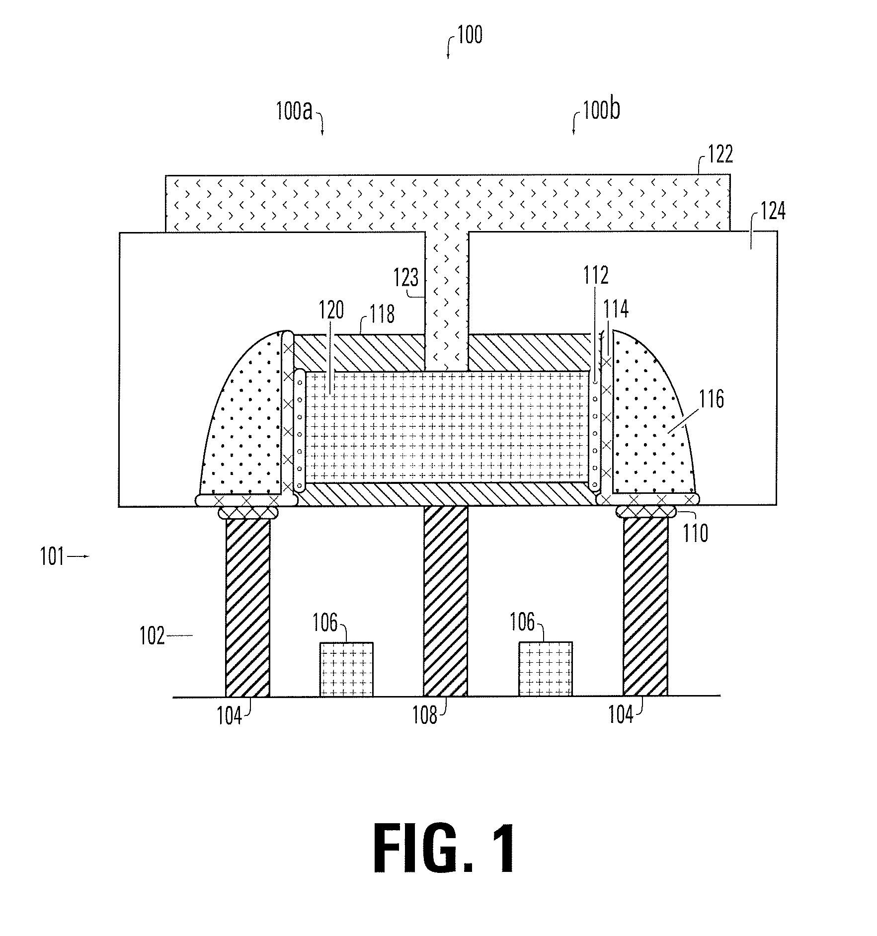
[0016]A detailed description of multi-bit memory cells, arrays of such memory cells, and methods for manufacturing such memory cells, is provided with reference to FIGS. 1-6.

[0017]FIG. 1 depicts an embodiment 100 of a memory cell incorporating memory elements 100a, 100b that respond to the requirements of the claims appended hereto. As is generally practiced in memory element designs, the memory element shown and discussed here is part of a larger memory circuit, in which memory elements 100a and 100b are components of memory cell 100. Memory cells are arrayed for controlled access, and a complete memory unit can hold a billion or more memory elements. The circuit arrangements apart from the memory element are outside the scope of this invention. A typical memory circuit can be seen in U.S. patent application Ser. No. 11 / 155,067, entitled “Thin Film Fuse Phase Change Ram and Manufacturing Method”, commonly owned with the application herein, which patent application is hereby incorpo...


PUM


Abstract

A memory device that selectably exhibits first and second logic levels. A first conductive material has a first surface with a first memory layer formed thereon, and a second conductive material has a second surface with a second memory layer formed thereon. A connective conductive layer joins the first and second memory layers and places the same in electrical contact. The structure is designed so that the first memory layer has a cross-sectional area less than that of the second memory layer.

Description

BACKGROUND OF THE INVENTION[0001]1. Field of the Invention[0002]The present invention relates to non-volatile memory devices, and more particularly to device suitable for constructing large-scale, ultra-compact memory systems.[0003]2. Description of Related Art[0004]The ever-increasing demand for stable, compact and reliable non-volatile memory, particularly for applications related to flash memory devices, has led to the introduction of a number of different devices. One highly useful technology has been resistive random access memory (RRAM), in which the memory element exhibits an ability to change between two or more states, each having a characteristic resistance level. The ability to move between such states is easily translated into an ability to display two resistance levels, which can easily be equated to logical values 0 and 1.[0005]A number of materials have shown an ability that allows their use in such memory applications. One example are the so-called chalcogenides, whi...

Claims


Application Information

Patent Timeline
Patent Type & Authority Applications(United States)
IPC IPC(8): G11C11/00
CPCB82Y10/00G11C11/5664G11C11/5678G11C11/5685G11C13/0004G11C13/0007G11C13/0014G11C13/0016G11C2213/31G11C2213/32G11C2213/34G11C2213/79H10B63/80H10N70/821H10N70/20H10N70/231H10N70/028H10N70/8828H10N70/8833
Inventor LAI, ERH-KUNHO, CHIAHUAHSIEH, KUANG YEU
Owner MACRONIX INT CO LTD
Why Eureka
Try Eureka