Packaging with base layers comprising alloy 42

Active Publication Date: 2008-05-01
TAIWAN SEMICON MFG CO LTD
View PDF11 Cites 27 Cited by
  • Summary
  • Abstract
  • Description
  • Claims
  • Application Information

AI Technical Summary

Benefits of technology

[0007]An advantageous feature of the present invention is that alloy 42 has a similar coefficient of therma

Problems solved by technology

Since semiconductor chips are typically small and fragile, they need to be packaged before being used.
The conventional packages suffer drawbacks.
First, forming solder bumps 6 involves a high cost.
The packaging process also suffers high

Method used


Image

  • Packaging with base layers comprising alloy 42
  • Packaging with base layers comprising alloy 42
  • Packaging with base layers comprising alloy 42

Examples


Embodiment Construction

[0011]The making and using of the presently preferred embodiments are discussed in detail below. It should be appreciated, however, that the present invention provides many applicable inventive concepts that can be embodied in a wide variety of specific contexts. The specific embodiments discussed are merely illustrative of specific ways to make and use the invention, and do not limit the scope of the invention.

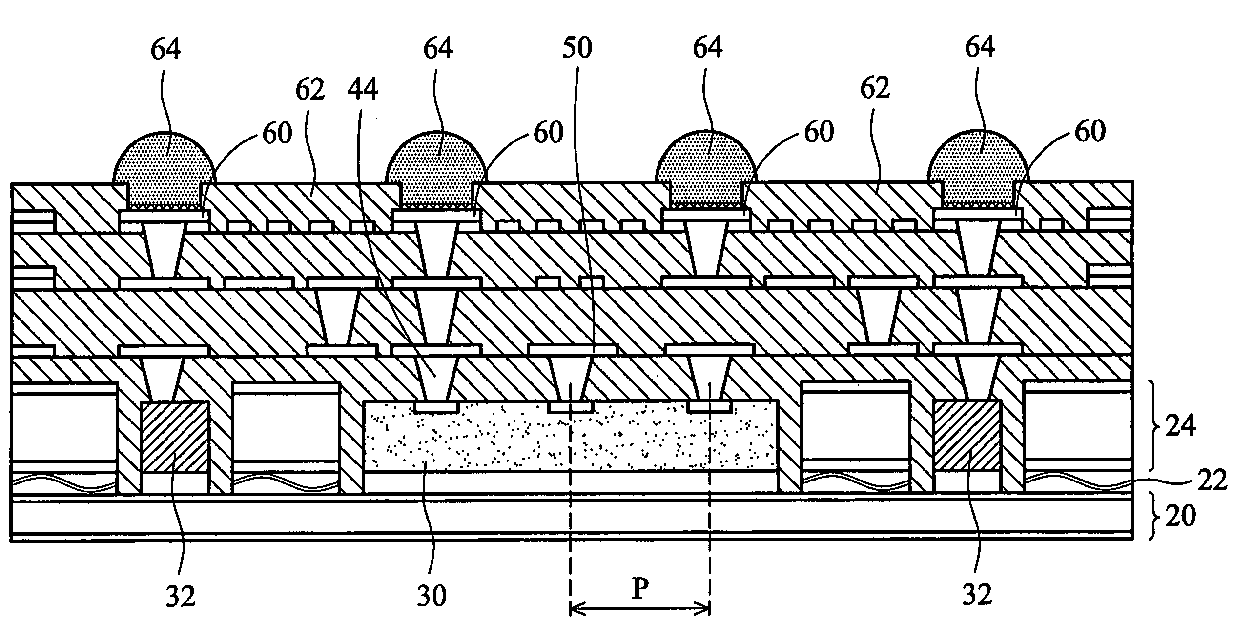
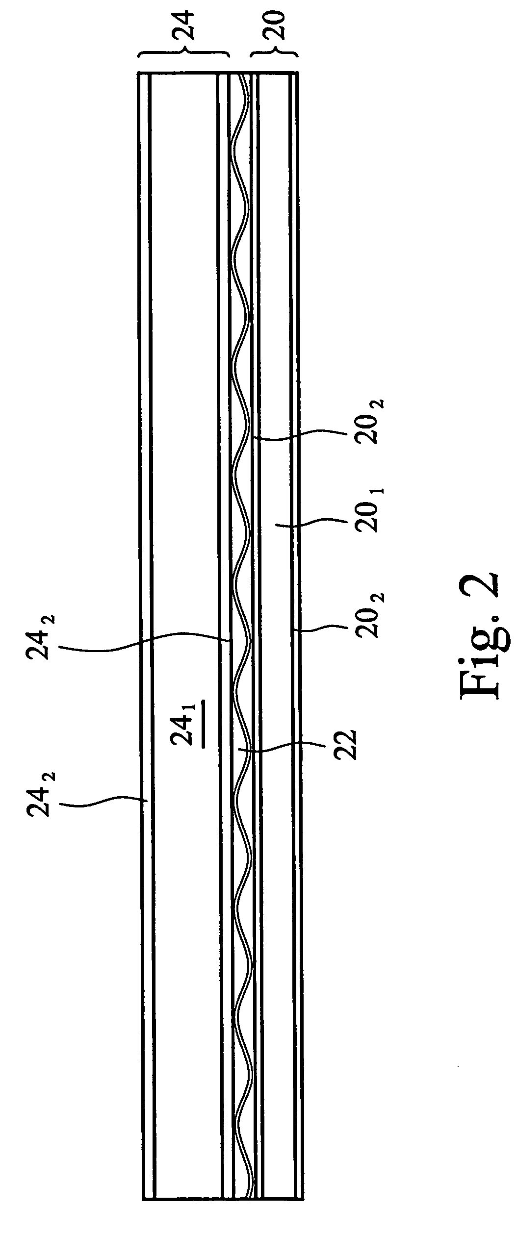
[0012]A novel packaging structure and methods for forming the same are provided. The intermediate stages of manufacturing an embodiment of the present invention are illustrated in FIGS. 2 through 10. Throughout the various views and illustrative embodiments of the present invention, like reference numbers are used to designate like elements.

[0013]FIG. 2 illustrates a starting structure that includes base layer 20, base layer 24 and an adhesive material 22. In an embodiment, base layer 20 includes a core 201 comprising “alloy 42,” which is a nickel iron alloy that will be disc...


PUM


Abstract

A semiconductor packaging structure is provided. The structure includes a base layer comprising alloy 42; die attached on a first side of the base layer; and an interconnect structure on the die, wherein the interconnect structure comprises vias and conductive lines connected to the die.

Description

TECHNICAL FIELD[0001]This invention relates generally to packaging of semiconductor chips, and more particularly to the structure and methods for embedding semiconductor chips into packages.BACKGROUND[0002]In the semiconductor industry, integrated circuits are typically formed on wafers, wherein a plurality of semiconductor chips on the same wafer is formed simultaneously. The semiconductor chips are then sawed from the wafers. Since semiconductor chips are typically small and fragile, they need to be packaged before being used.[0003]FIG. 1 illustrates a conventional package, which includes a semiconductor chip (die) 2 bonded to a package substrate 4, for example, through solder bumps 6. Package substrate 4 includes a core 8 and a plurality of interconnect layers built up on both sides of core 8. Die 2 and core 8 are separated by interconnect layers. On a side of core 8 opposite the side where die 2 is attached, ball grid array (BGA) balls 10 are formed for connecting package substr...

Claims


Application Information

Patent Timeline
IPC IPC(8): H01L23/48
CPCH01L23/142H01L2924/19105H01L23/5389H01L23/562H01L24/18H01L24/82H01L2224/18H01L2224/82039H01L2224/92244H01L2924/01013H01L2924/01015H01L2924/01029H01L2924/01033H01L2924/01074H01L2924/01078H01L2924/14H01L2924/15311H01L2924/19041H01L2924/30107H01L2924/01019H01L2924/01047H01L2924/014H01L2224/16225H01L2224/12105H01L2224/32245H01L2224/73267H01L23/49866H01L24/05H01L24/19H01L2224/04105H01L2224/05022H01L2224/05124H01L2224/05139H01L2224/05147H01L2224/05155H01L2224/05568H01L2224/05624H01L2224/05639H01L2224/05647H01L2224/05655H01L2924/3511H01L2924/00014H01L2924/013
Inventor WU, GENE
Owner TAIWAN SEMICON MFG CO LTD
Why Eureka
Try Eureka