Optical device module, fabrication method thereof, optical device unit and fabrication method thereof
a technology of optical devices and optical devices, applied in the field of optical device modules, can solve the problems of deteriorating workability, increasing production costs, and difficulty in fabricating solid-state image sensing device modules, and achieve the effect of increasing production costs and high accuracy
- Summary
- Abstract
- Description
- Claims
- Application Information
AI Technical Summary
Benefits of technology
Problems solved by technology
Method used
Image

Examples
first embodiment
—Solid-State Image Sensing Device Module—
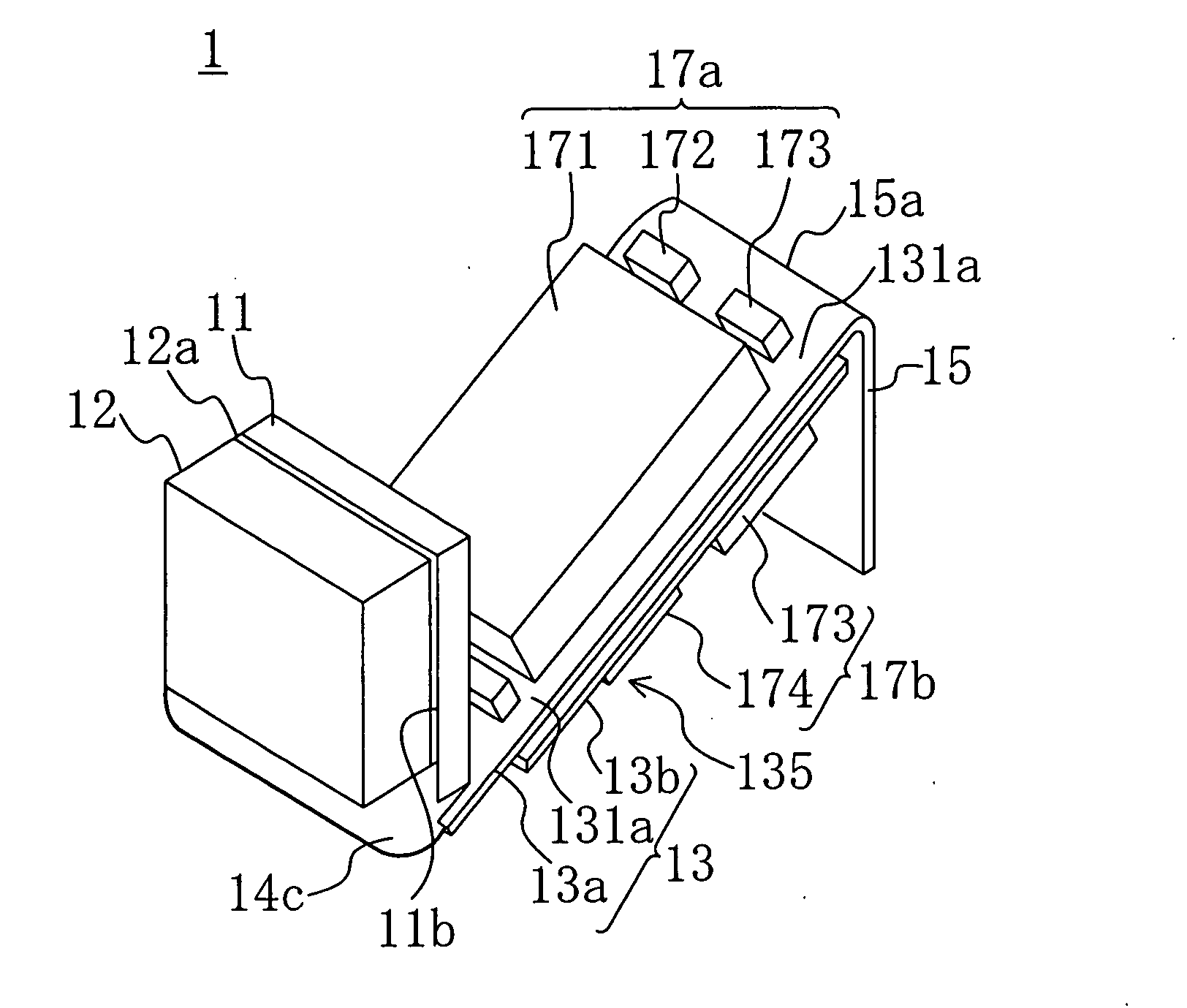
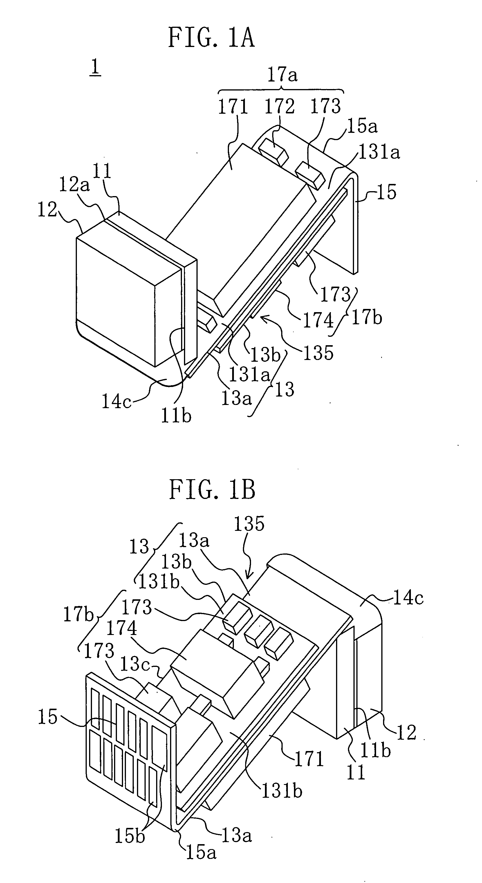
[0045]FIG. 1(a) is a conceptual perspective view showing the structure of a solid-state image sensing device module (optical device module) 1 according to a first embodiment of the present invention and FIG. 1(b) is a conceptual perspective view of the solid-state image sensing device module in FIG. 1(a) when viewed from below.
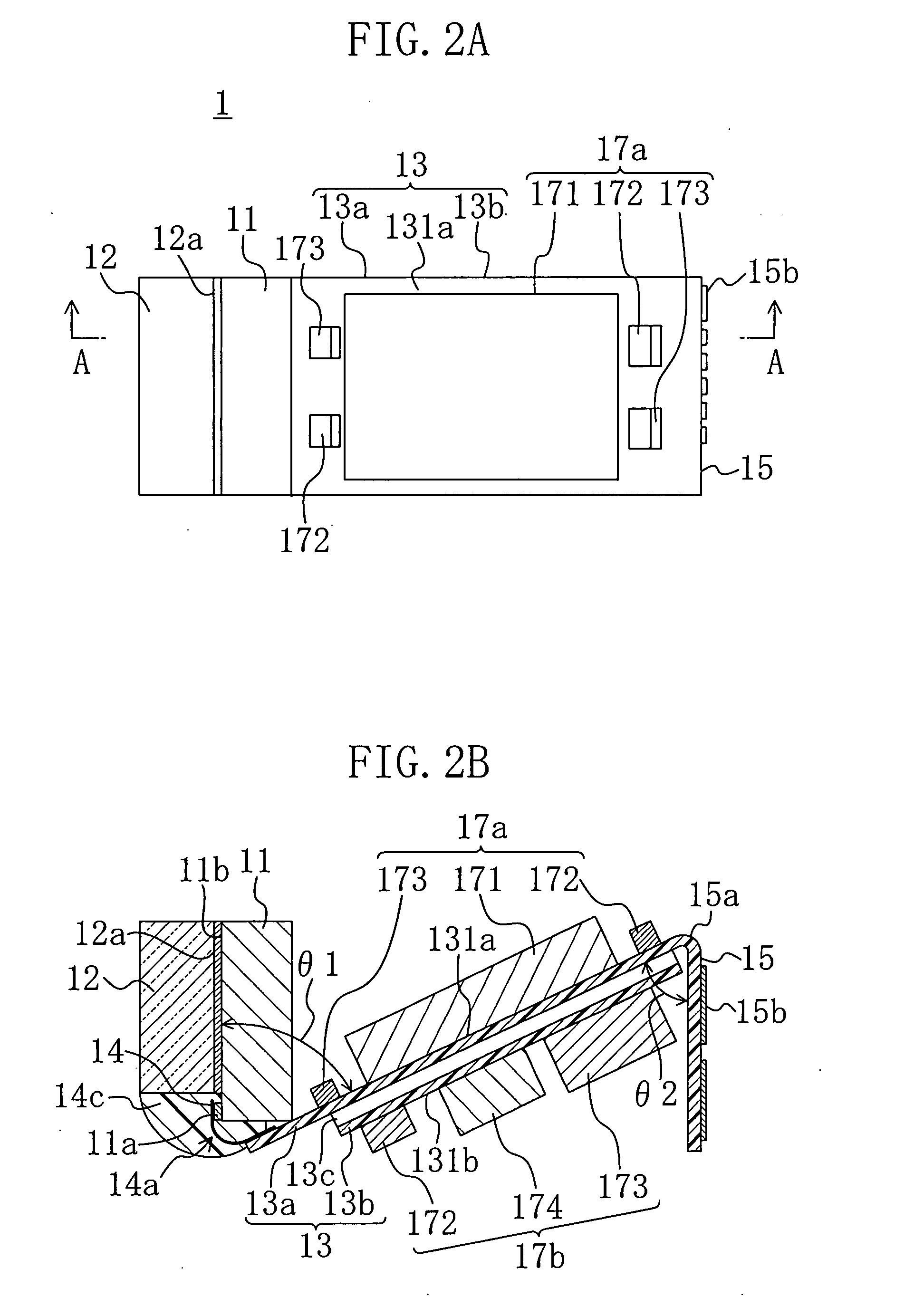
[0046]FIG. 2(a) is a conceptual plan view showing the structure of the solid-state image sensing device module 1 according to the first embodiment and FIG. 2(b) is a conceptual cross-sectional view taken along the line A-A of FIG. 2(a).
[0047]As shown in FIGS. 1 and 2, the solid-state image sensing device module 1 includes a solid-state image sensing device (optical device) 11, such as a CCD (charge-coupled image sensing device), and a flexible substrate (for example, polyimide resin substrate) 13 having flexibility. The solid-state image sensing device module 1 further includes electronic componentry 17a mounted on a su...
second embodiment
[0075]FIG. 7(a) is a conceptual plan view showing the structure of a solid-state image sensing device module 3 according to a second embodiment of the present invention and FIG. 7(b) is a conceptual cross-sectional view taken along the line A-A of FIG. 7(a). In these figures, the same components and parts as in FIG. 2 are partly designated by the same reference numerals and partly not given the reference numerals. This embodiment is different from the first embodiment in that a flexible substrate 33 is a double-sided wiring substrate on which wiring patterns (not shown) are formed on both the surfaces (both sides), a via hole (not shown) is formed in a substrate body 33a of a mounting part 335 of the flexible substrate 33 and a second set of electronic componentry is mounted on the other surface of the mounting part 335. Specifically, the first set of electronic componentry 17a and the second set of electronic componentry 17b are mounted on one surface of the flexible substrate 33 a...
third embodiment
[0078]FIG. 8 is a conceptual cross-sectional view showing the structure of a solid-state image sensing device module 4 according to a third embodiment of the present invention. The same components and parts as in FIG. 2 are partly designated by the same reference numerals and partly not given the reference numerals. This embodiment is different from the first embodiment in that metal leads (wirings) are disposed on the film at a contact terminal part 44 and a first bent part 44a. The other points are the same as in the first embodiment and, therefore, a description thereof is not given.
[0079]As shown in FIG. 8, the solid-state image sensing device module 4 is formed with no film holes under the contact terminal part 44 and the first bent part 44a of a flexible substrate 43 and, therefore, the contact terminal part 44 and the first bent part 44a are supported by the film. Specifically, the contact terminal part 44 is provided on one surface (substrate principal surface) 431a of a fir...
PUM
 Abstract
Description
Claims
Application Information