Nanostructures and methods for manufacturing the same

a nanostructure and nanotechnology, applied in nanotechnology, photovoltaic energy generation, crystal growth process, etc., can solve the problems of difficult control of size and surface coverage separately, virtually impossible to achieve a low coverage, and may provoke a considerable change in the separation of energy states

Inactive Publication Date: 2008-05-08
QUNANO
View PDF58 Cites 31 Cited by
  • Summary
  • Abstract
  • Description
  • Claims
  • Application Information

AI Technical Summary

Benefits of technology

[0014] Further, the invention includes a technique for the synthesis of size-selected, epitaxial nano-whiskers, grown on a crystalline substrate. As catalysts, size-selected gold aerosol particles are used, which enables the surface coverage to be varied completely independently of the whisker diameter. The whiskers were rod shaped, with a uniform diameter between 10 and 50 nm, correlated to the size of the catalytic seed. By the use of nano-manipulation of the aerosol particles, individual nano-whiskers can be nucleated in a controlled manner at specific positions on a substrate with accuracy on the nm level. The method of the invention enhances width control of the whisker by virtue of choice of nanoparticle. The nanoparticle may be an aerosol or a liquid alloy on the substrate may be made by starting from gold rectangles formed on the substrate which when melted form accurate diameter balls. Other materials may be used instead of gold as the seed particle, e.g. Gallium.
[0031] The precision of formation of the nanowhisker enables production of devices relying on quantum confinement effects, in particular a resonant tunneling diode. Thus, an RTD has been developed wherein the emitter, collector and the central quantum dot are made from InAs and the barrier material from InP. Ideal resonant tunneling behavior, with peak-to-valley ratios of up to 50:1, was observed at low temperatures.
[0036] Alternatively, in a method which may be better suited to mass-production, the nanowhiskers may be left on the substrate, with their base ends having been formed on an electrical contact. Once formed, the nanowhiskers may be encapsulated in a resin or glassy substance, and then contact pads may be formed over the surface of the encapsulation in contact with the free ends of the nanowhiskers. To assist in this, the catalytic particle melt, towards the end of the formation of the nanowhisker, may have extra conductive substances injected into it, so as to improve the electrical contact with the bond pads.
[0038] Light emitting diodes are well suited to the present invention, since it is possible to construct them with an emission wavelength which can be selected at will from a continuous range of wavelengths over the UV, visible, and infrared regions.
[0050] In a further modification, microscopic V-grooves are formed in the upper surface of the silicon surface, for example <111> etchings in a <100> substrate. The seed particle forming areas are formed on the surfaces of the V-grooves, whereby the nanowhiskers grow at an angle to the substrate, and cross one another at the grooves. This makes for a more efficient growth of the epitaxial layer from the nanowhisker nucleation centres. Further, grain boundaries between domain areas with different growth phases are avoided; which has been a problem with prior processes.
[0056] In one aspect a substrate, for example of silicon, has a matrix of electrical contact areas formed on one surface. On each contact area, one, or a number, of nanowhiskers are formed from, for example, gold catalyst particles so as to be upstanding from the substrate's surface. Each nanowhisker, or group of nanowhiskers may therefore be individually addressable by electrical signals. Such a structure may make contact with the end of a nerve or perhaps the nerves in the retina of an eye, and the electrodes may be activated so as to provide a repairing or artificial function for enabling the nerve. Thus for example, when applied in the retina of an eye, the structure may overcome certain blindness problems.

Problems solved by technology

In particular, a small variation of the width of the whisker may provoke a considerable change in the separation of the energy states due to the quantum confinement effect.
With this technique, it is difficult to control the size and surface coverage separately, and it is virtually impossible to achieve a low coverage.
The correlation between film thickness and whisker thickness was not straightforward, since the whisker width also depended on growth temperature, and there were even signs of a temperature-dependent equilibrium size of the Au particles.
Despite progress, research has been frustrated by a lack of control of the conductivity-type of CNTs and an inability to form 1D heterostructures in a controlled manner.
In the studies of devices fabricated by this bottom-up technique, 100-200 nm diameter columns have been observed, however, with rather disappointing electrical characteristics and peak-to-valley currents at best around 1.1:1.

Method used


Image

  • Nanostructures and methods for manufacturing the same
  • Nanostructures and methods for manufacturing the same
  • Nanostructures and methods for manufacturing the same

Examples


example 1

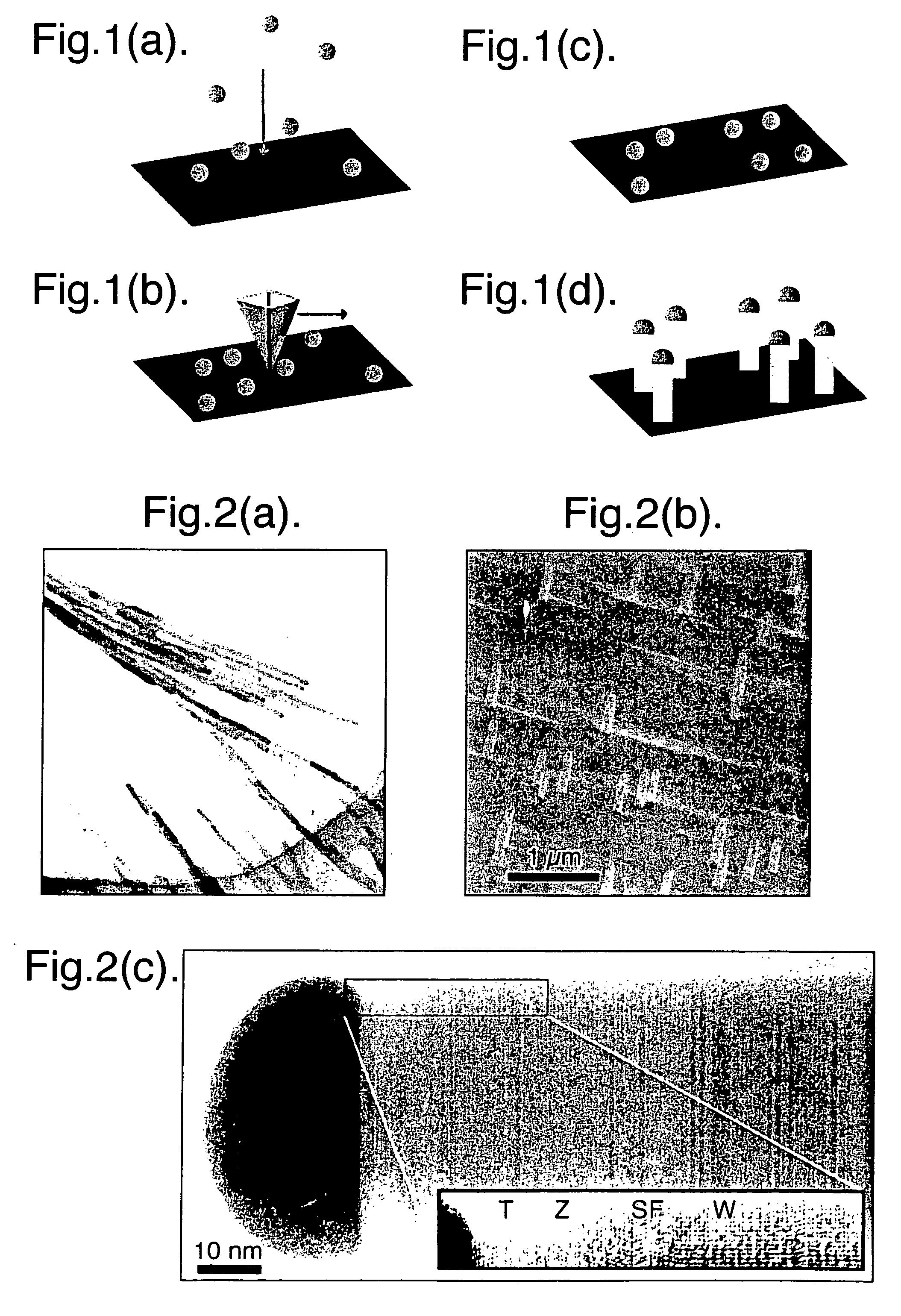
[0110]FIGS. 1 and 3 show whiskers of predetermined sizes grown from several III-V materials, in particular, GaAs whiskers with widths between 10 and 50 nm. These whiskers can be grown rod shaped with a uniform diameter, in contrast to earlier reports on epitaxially grown nano-whiskers, which tended to be tapered, narrowing from the base towards the top. As catalysts, size-selected gold aerosol particles were used, whereby the surface coverage can be varied independently of the whisker diameter.

[0111] The whisker width in general is slightly larger than the seed particle diameter. This is mainly due to two factors: First, the gold particle incorporates Ga and possibly As from the substrate, which makes the particle grow. Second, when the particle melts, the base diameter of the liquid cap will be determined by the wetting angle between the alloy and the substrate surface. Simple assumptions give a widening of up to 50%, depending on temperature and particle diameter, and introduce a...

example 2

[0118] Conditions for growth of nanowhiskers allow the formation of abrupt interfaces and heterostructure barriers of thickness from a few monolayers to 100s of nanometers, thus creating a one-dimensional landscape along which the electrons move. The crystalline perfection, the quality of the interfaces, and the variation in the lattice constant are demonstrated by high-resolution transmission electron microscopy, and the conduction band off-set of 0.6 ev is deduced from the current due to thermal excitation of electrons over an InP barrier.

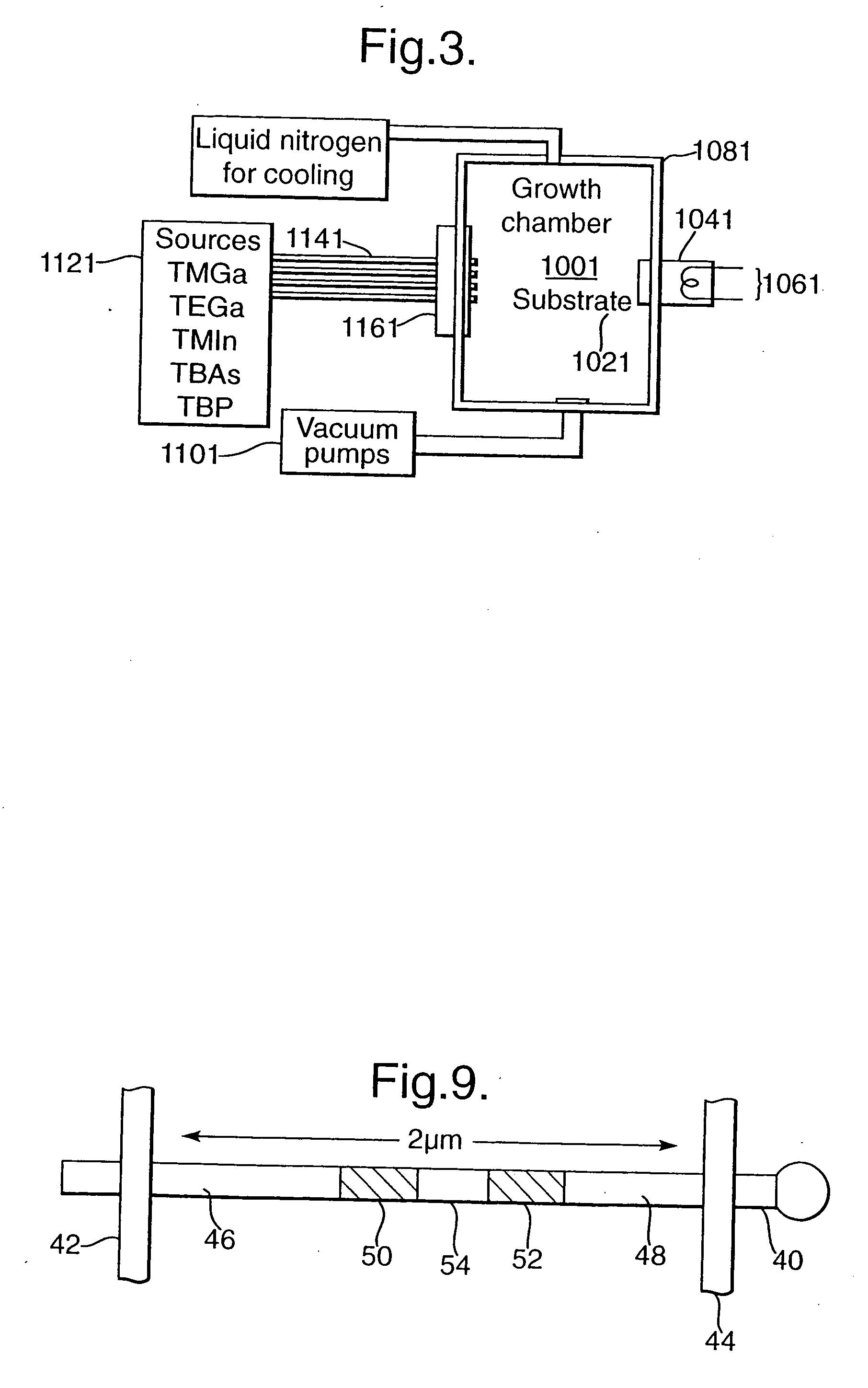
[0119] In this method, the III-V whiskers are grown by the vapor-liquid-solid growth mode, with a gold nanoparticle catalytically inducing growth, in the manner described above. Growth occurs in an ultrahigh vacuum chamber 100, FIG. 3, designed for chemical beam epitaxy (CBE). The rapid alteration of the composition is controlled by the supply of precursor atoms into the eutectic melt, supplied as molecular beams into the ultrahigh vacuum chambe...


PUM

PropertyMeasurementUnit
thicknessaaaaaaaaaa
sizeaaaaaaaaaa
diameteraaaaaaaaaa

Abstract

A resonant tunneling diode, and other one dimensional electronic, photonic structures, and electromechanical MEMS devices, are formed as a heterostructure in a nanowhisker by forming length segments of the whisker with different materials having different band gaps.

Description

CROSS-REFERENCE TO RELATED APPLICATIONS [0001] This application is a Divisional of U.S. application Ser. No. 10 / 613,071, filed on Jul. 7, 2003, which claims the benefit of the priority of U.S. Provisional Application No. 60 / 393,835, filed Jul. 8, 2002, and of U.S. Provisional Application No. 60 / 459,982, filed on Apr. 4, 2003, each of which is incorporated herein by reference in its entirety.BACKGROUND OF THE INVENTION [0002] 1. Field of the Invention [0003] This invention relates generally to structures, essentially in one-dimensional form, and which are of nanometer dimensions in their width or diameter, and which are commonly known as nanowhiskers, nanorods, nanowires, nanotubes, etc.; for the purposes of this specification, such structures will be termed “one-dimensional nanoelements”. More specifically, but not exclusively, the invention relates to nanowhiskers, and to methods of forming nanowhiskers. [0004] 2. Brief Description of the Prior Art [0005] The basic process of whisk...

Claims


Application Information

Patent Timeline
Patent Type & Authority Applications(United States)
IPC IPC(8): H01L31/072B82B3/00B82B1/00C30B11/00C30B11/12C30B25/00C30B25/02C30B25/14C30B25/18H01J31/12H01L21/331H01L29/06H01L29/20H01L29/737H01L29/88H01L31/068H01L31/10
CPCB82Y10/00H01L31/048C30B11/12C30B25/00C30B25/02C30B25/14C30B25/18C30B25/183C30B29/403C30B29/406C30B29/605H01L29/0665H01L29/0673H01L29/068H01L29/20H01L29/66318H01L29/7371H01L29/882C30B11/00H01L31/035227H01L31/022466Y02E10/544H01L33/04Y10S977/762Y10S977/763H01L31/068Y02E10/547B82B3/00B82B1/00B82Y40/00
Inventor SAMUELSON, LARS IVAROHLSSON, BJORN JONAS
Owner QUNANO
Why Eureka
Try Eureka