Method and Manufacturing Thin Film Photovoltaic Modules
- Summary
- Abstract
- Description
- Claims
- Application Information
AI Technical Summary
Problems solved by technology
Method used
Image
Examples
example
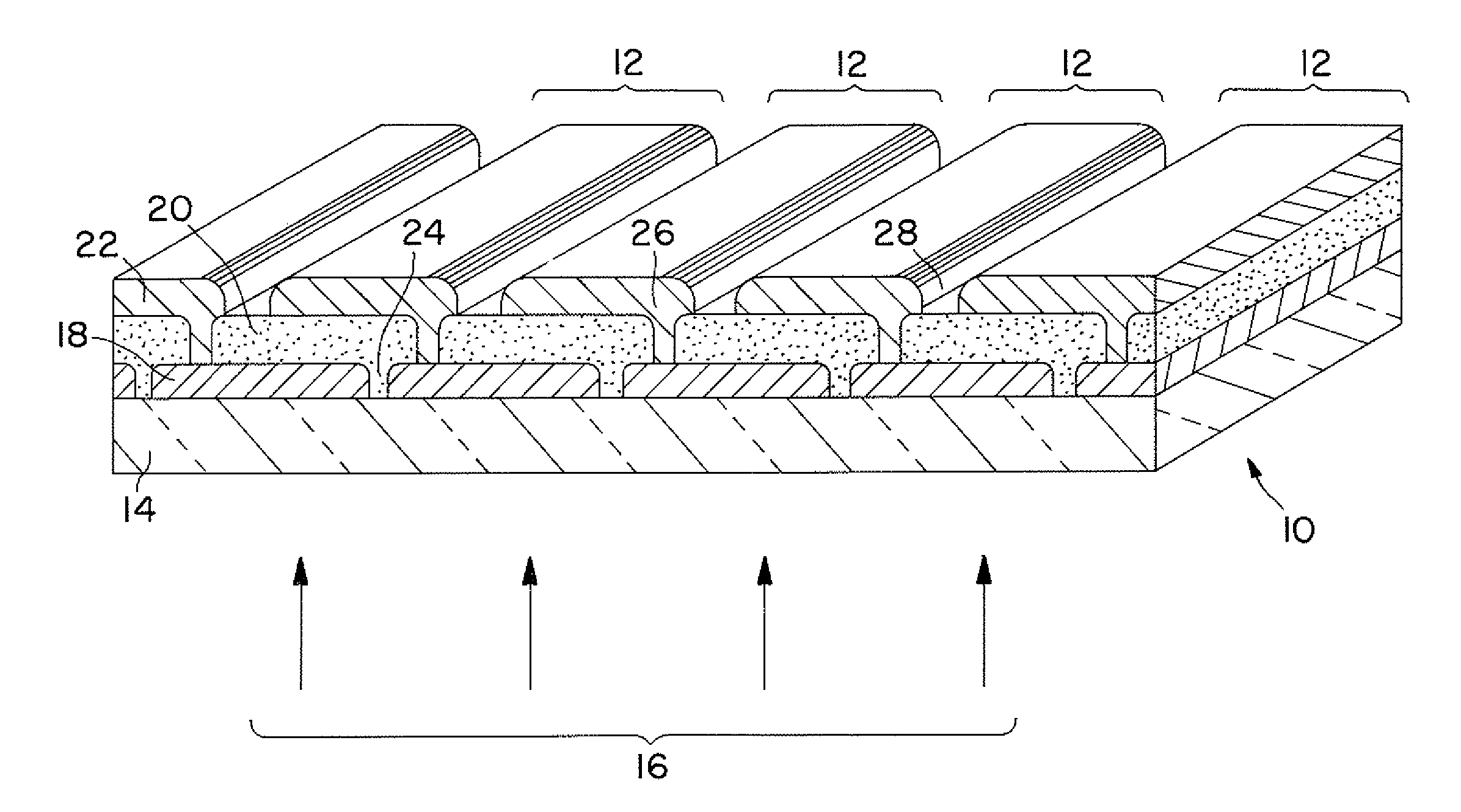
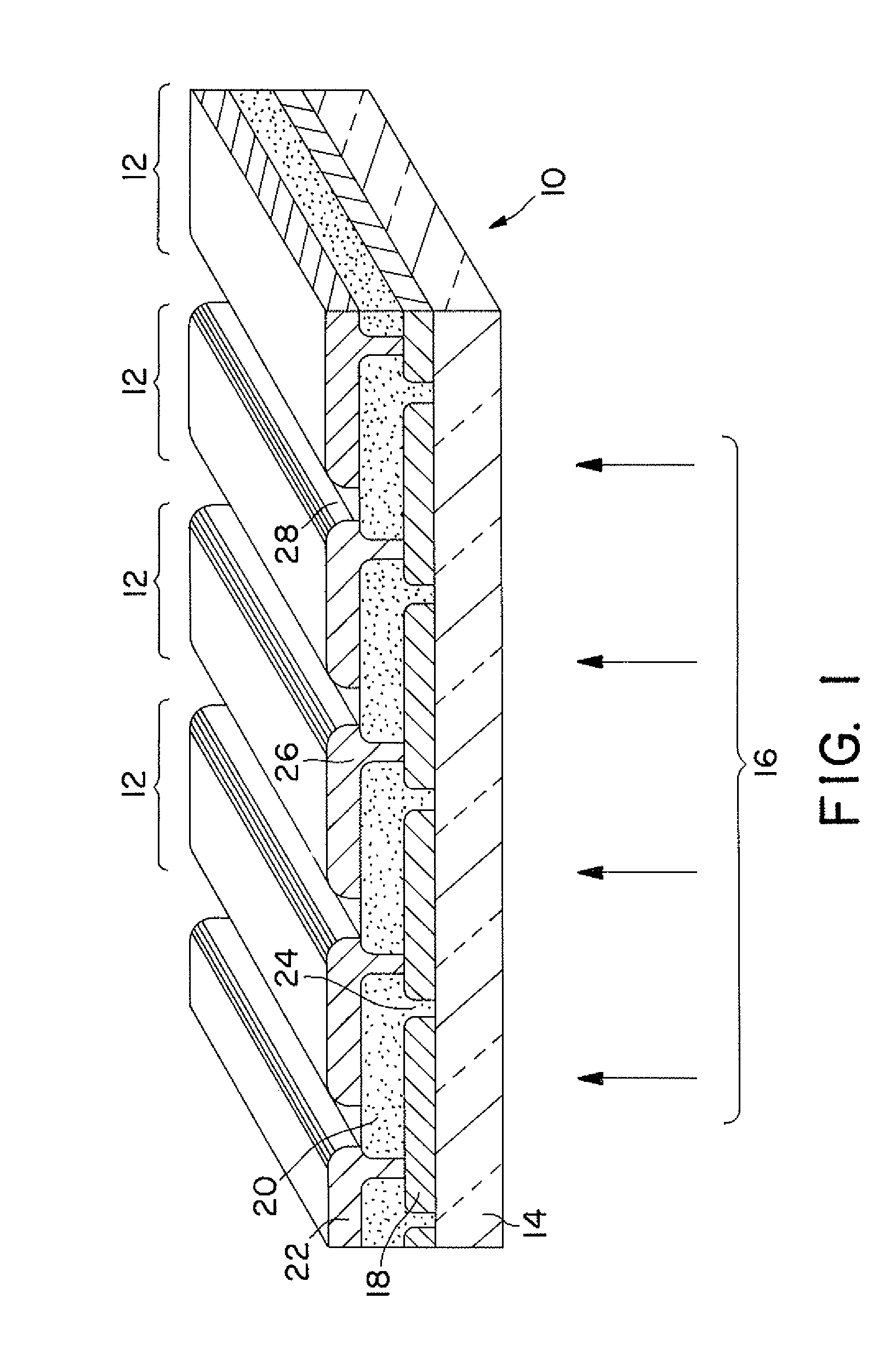
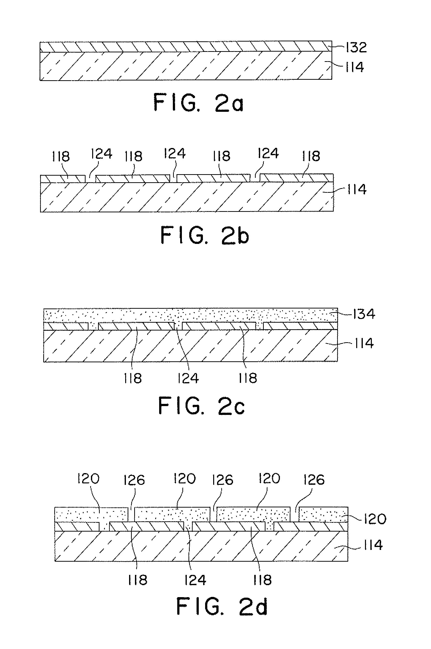
[0064] Using the apparatus as shown in FIG. 5, a 48 inch long by 26 inch wide glass plate ⅛ inch in thickness having a 0.6-0.8 micrometer layer of tin oxide doped with fluorine is scribed to remove the tin oxide using a Nd:YVO4 laser operating at 32 nm at 30 kHz reprate delivering an average laser power of about 5 W by scanning the laser over the tin oxide laser at a rate of about 1 meter per second. The scribes are set parallel to the length of the glass plate and are spaced from each other about 9 mm and are about 50 micrometers in width. Such scanning results in a series of strips of tin oxide layer approximately 9 mm wide separated by 50 micrometer wide scribes across the entire surface of the glass substrate. Bus bars are added by placing a bead of silver-containing frit paste along the length of the outside edges of the first an last strip of conductive oxide. The beads are extended to a point near the center of one end of the substrate to function as positive and negative ter...
PUM
| Property | Measurement | Unit |
|---|---|---|
| Speed | aaaaa | aaaaa |
| Area | aaaaa | aaaaa |
| Size | aaaaa | aaaaa |
Abstract
Description
Claims
Application Information


