Group-III nitride based laser diode and method for fabricating same

Active Publication Date: 2008-05-15
CREELED INC
View PDF15 Cites 1 Cited by
  • Summary
  • Abstract
  • Description
  • Claims
  • Application Information

AI Technical Summary

Benefits of technology

[0010]The present invention is generally directed to laser diode epitaxial structure having improved operating characteristics and improved reliability, and methods for fabricating th

Problems solved by technology

Group-III nitride laser diodes can require relatively high threshold currents and voltages to reach laser radiation because of optical and electrical inefficiencies.
These elevated current and voltage levels can result in heat being generated during laser diode operation.
Driving many current Group-III based laser diodes with a CW having the t

Method used


Image

  • Group-III nitride based laser diode and method for fabricating same
  • Group-III nitride based laser diode and method for fabricating same
  • Group-III nitride based laser diode and method for fabricating same

Examples


Example

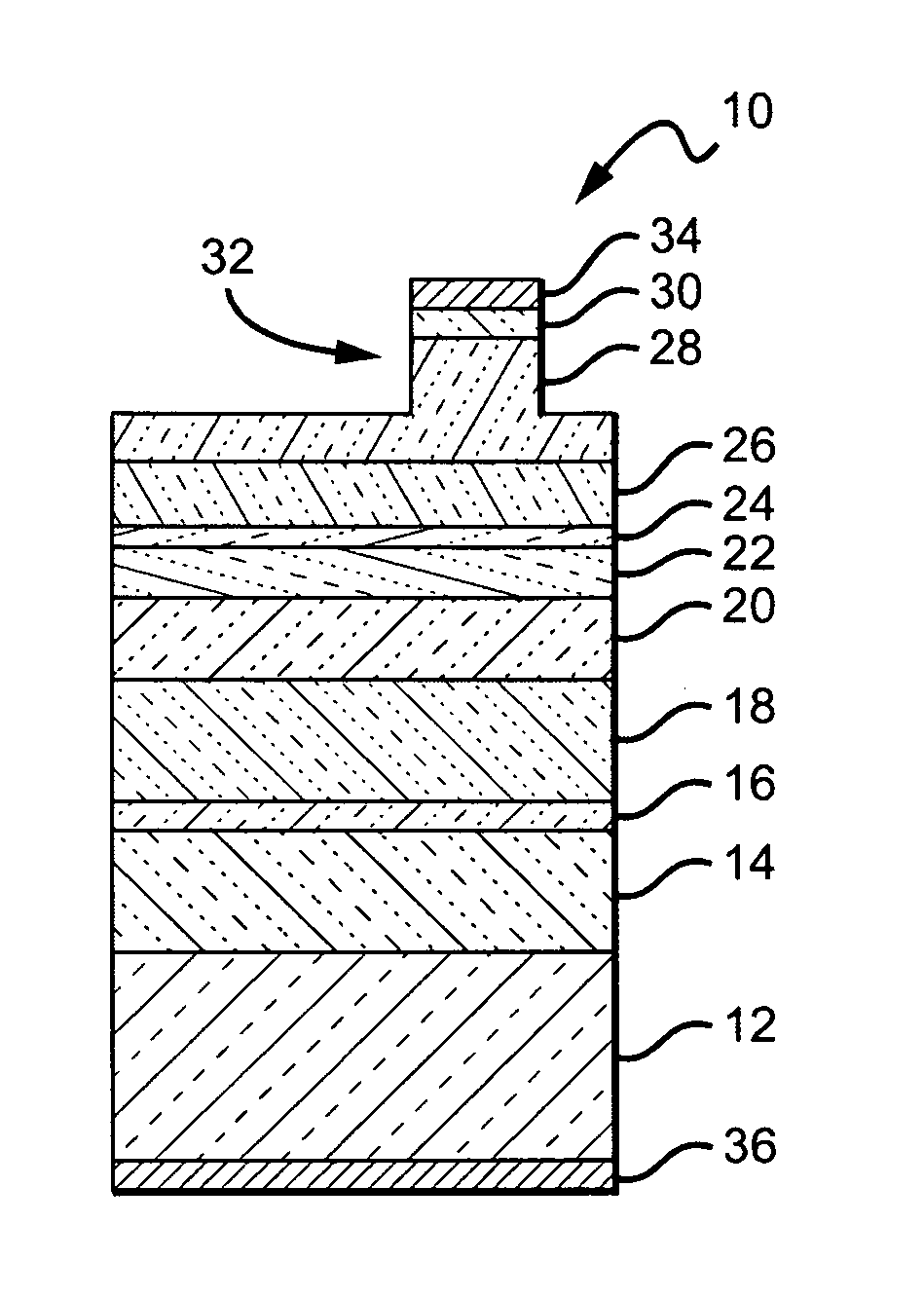
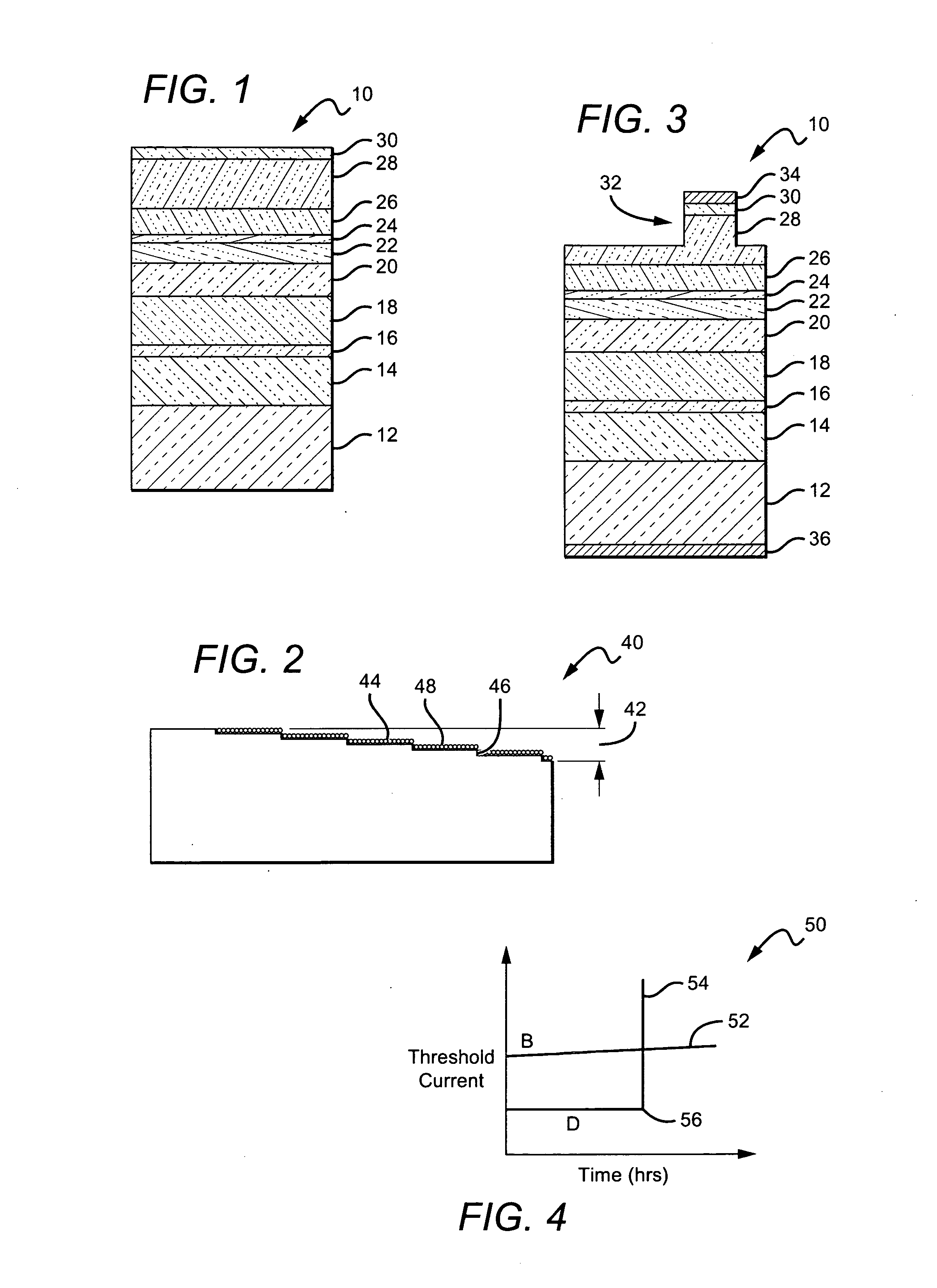
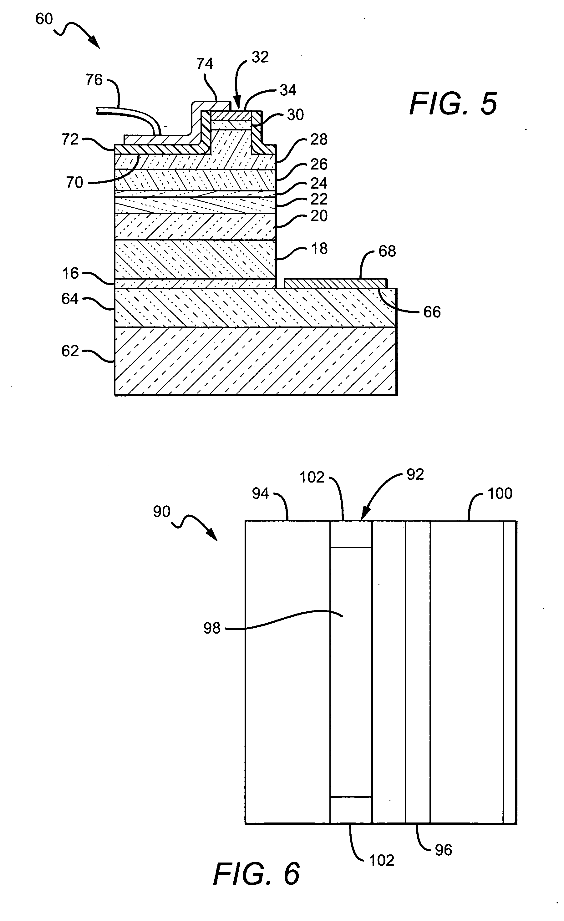
[0020]The present invention provides high reliability, high output power nitride-based laser diode characterized by reduced threshold current densities and reduced threshold voltages. The present invention is particularly adapted for laser diodes having a ridge for optical and electrical confinement, with the ridge being etched to level in the laser diode structure that allows for reduced threshold current operation while at the same time allowing for reliable lifetime operation. The present invention is also directed to additional laser diode structural and manufacturing improvements that further enhance laser diode operation.

[0021]The present invention is described herein with reference to certain embodiments but it is understood that the invention can be embodied in many different forms and should not be construed as limited to the embodiments set forth herein. It is also understood that when an element or component is referred to as being “on”, “connected to” or “coupled to” ano...


PUM


Abstract

A laser diode comprising a first separate confinement heterostructure and an active region on the first separate confinement heterostructure. A second separate confinement heterostructure is on the active region and one or more epitaxial layers is on the second separate confinement heterostructure. A ridge is formed in the epitaxial layers with a first mesa around the ridge. The first mesa is 0.1 to 0.2 microns above the second confinement heterostructure.

Description

BACKGROUND OF THE INVENTION[0001]1. Field of the Invention[0002]This invention relates to laser diodes, and more particularly to nitride based semiconductor laser diodes and methods for fabricating same.[0003]2. Description of the Related Art[0004]A laser is a device that produces a beam of coherent light as a result of stimulated emission. Light beams produced by lasers can have high energy because of their single wavelength, frequency, and coherence. A number of materials are capable of producing a lasing effect and include certain high-purity crystals (such as ruby), semiconductors, certain types of glass, certain gasses including carbon dioxide, helium, argon and neon, and certain plasmas.[0005]More recently there has been increased interest in lasers made of semiconductor materials. These devices typically have a smaller size, lower cost, and have other related advantages typically associated with semiconductor devices. Semiconductor lasers are similar to other lasers in that t...

Claims


Application Information

Patent Timeline
IPC IPC(8): H01S5/20H01L21/00
CPCB82Y20/00H01S5/0021H01S5/0202H01S5/2009H01S5/2081Y10T428/12875H01S5/3063H01S5/3216H01S5/34333H01S2304/00H01S5/22
Inventor DENBAARS, STEVENNAKAMURA, SHUJIHANSEN, MONICA
Owner CREELED INC
Why Eureka
Try Eureka