Method to reduce junction leakage through partial regrowth with ultrafast anneal and structures formed thereby

a microelectronic device and partial regrowth technology, applied in the direction of semiconductor devices, electrical apparatus, transistors, etc., can solve the problem of damage to the implanted region of the ion implanted region

Inactive Publication Date: 2008-05-29
INTEL CORP
View PDF5 Cites 35 Cited by
  • Summary
  • Abstract
  • Description
  • Claims
  • Application Information

AI Technical Summary

Problems solved by technology

In some cases, the ion implanted region may be dama...

Method used


Image

  • Method to reduce junction leakage through partial regrowth with ultrafast anneal and structures formed thereby
  • Method to reduce junction leakage through partial regrowth with ultrafast anneal and structures formed thereby
  • Method to reduce junction leakage through partial regrowth with ultrafast anneal and structures formed thereby

Examples


Embodiment Construction

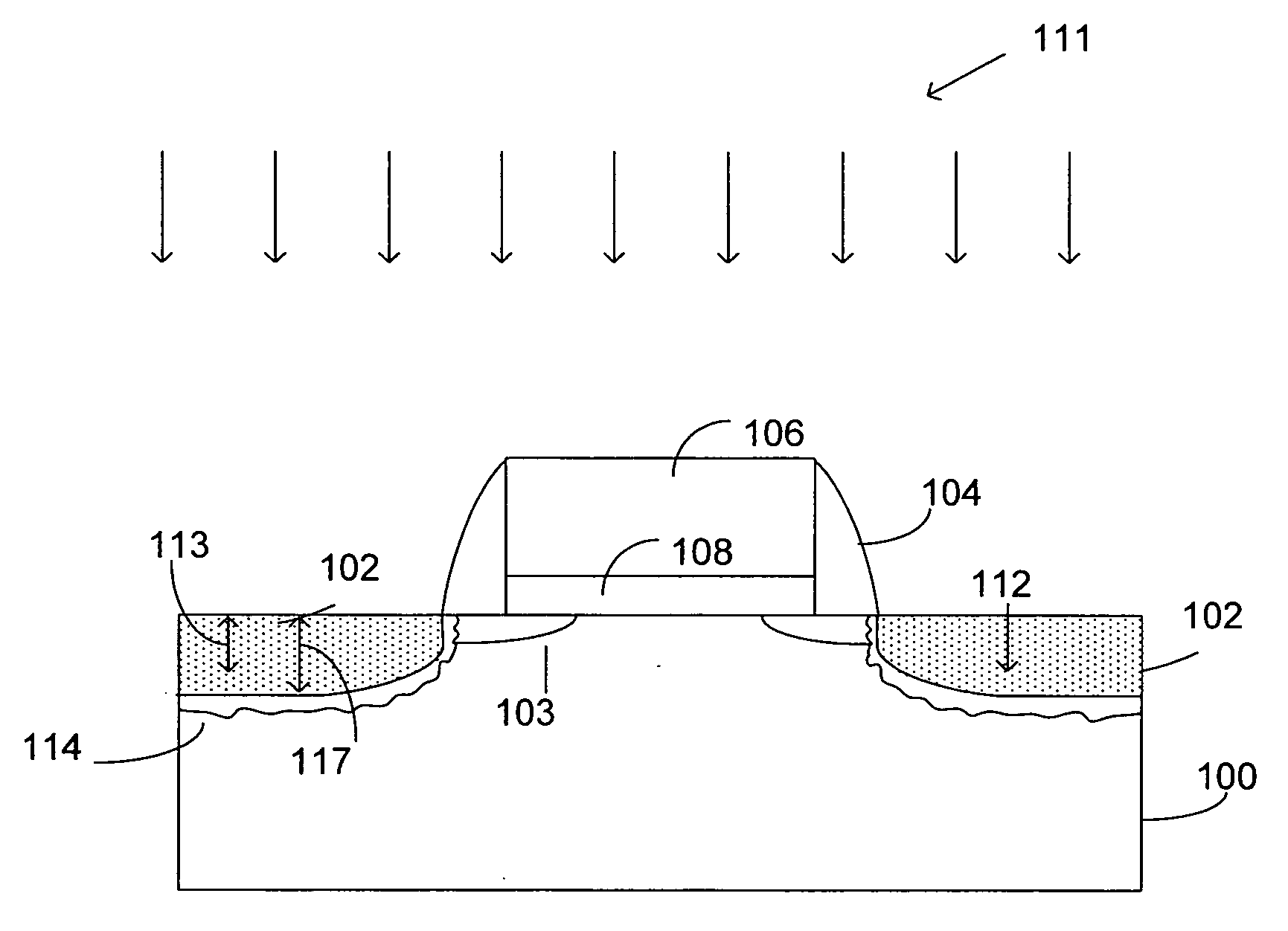
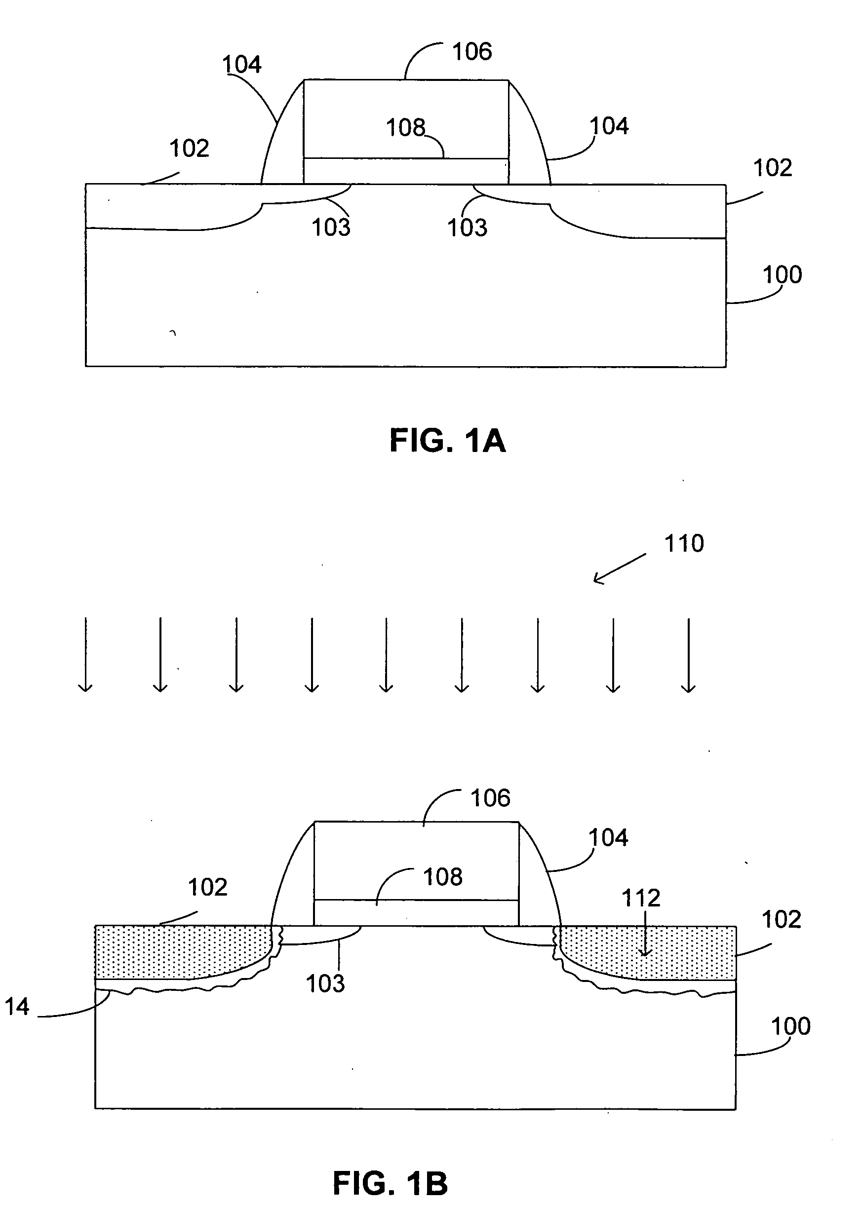
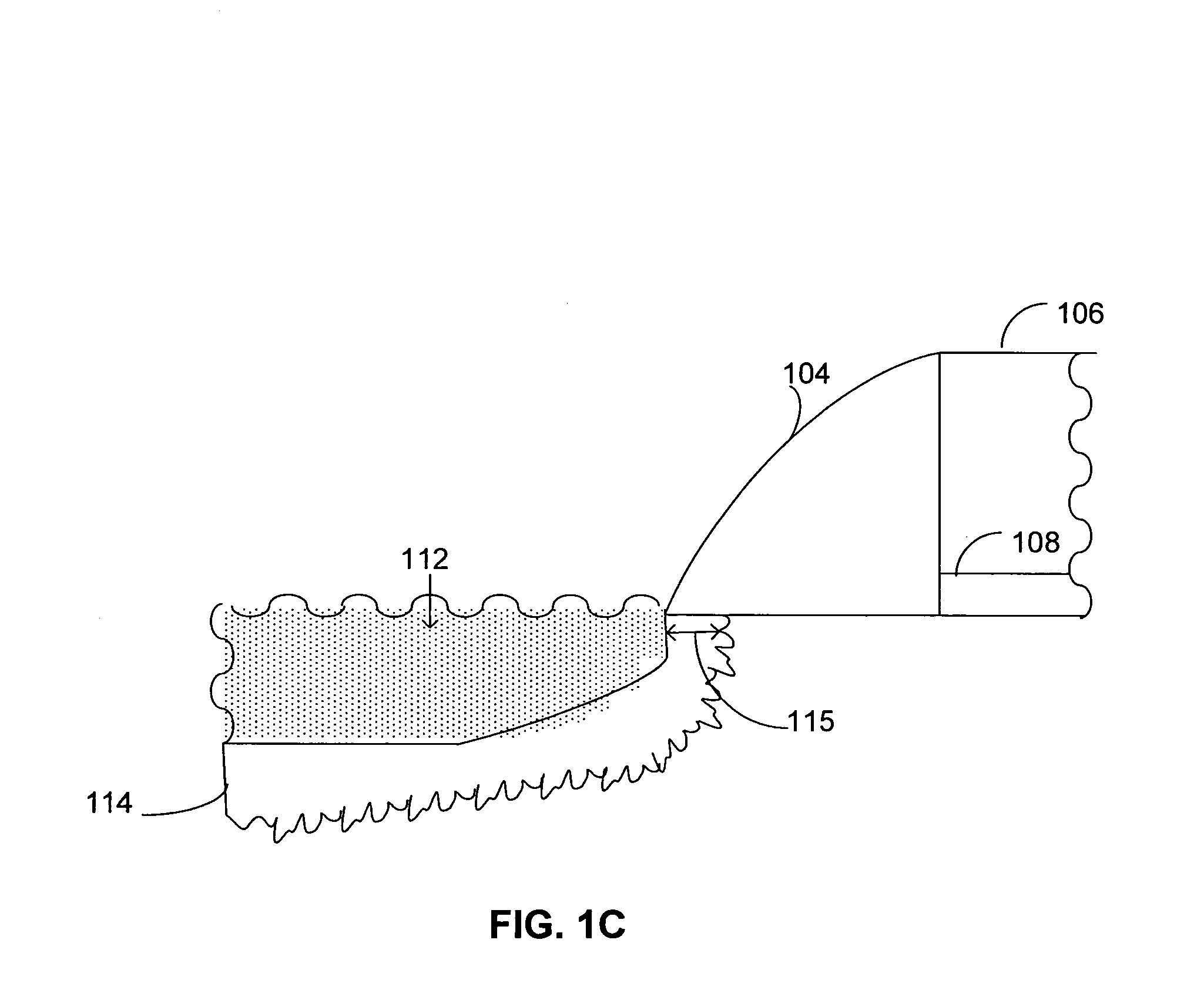
[0006]In the following detailed description, reference is made to the accompanying drawings that show, by way of illustration, specific embodiments in which the invention may be practiced. These embodiments are described in sufficient detail to enable those skilled in the art to practice the invention. It is to be understood that the various embodiments of the invention, although different, are not necessarily mutually exclusive. For example, a particular feature, structure, or characteristic described herein, in connection with one embodiment, may be implemented within other embodiments without departing from the spirit and scope of the invention. In addition, it is to be understood that the location or arrangement of individual elements within each disclosed embodiment may be modified without departing from the spirit and scope of the invention. The following detailed description is, therefore, not to be taken in a limiting sense, and the scope of the present invention is defined ...


PUM


Abstract

Methods and associated structures of forming a microelectronic device are described. Those methods may include creating an amorphous region in source/drain regions of a substrate by ion implantation with an electrically neutral dopant, annealing with a first anneal that removes defects without completely re-crystallizing the amophous region, ion implantation of electrically active dopant to a depth shallower than the remaining amorphous region, followed by a second anneal.

Description

BACK GROUND OF THE INVENTION[0001]One concern with the process of forming a microelectronic device, such as a device utilizing transistors, for example, involves the step of adding electrically active dopants to the junctions. One method of adding dopants involves the ion implantation of such dopant ions into the surface of a material, such as a semiconductor material, for example. After ion implantation, the dopants may be annealed at a high temperature to remove defects that may be present in the material and to place the dopants into substitutional lattice sites. In some cases, the ion implanted region may be damaged enough to convert the lattice into an amorphous layer. The manner in which the amorphous layer may be re-grown (i.e., re-crystallized) can have a large impact on the final electrical characteristics of the transistor.BRIEF DESCRIPTION OF THE DRAWINGS[0002]While the specification concludes with claims particularly pointing out and distinctly claiming that which is reg...

Claims


Application Information

Patent Timeline
IPC IPC(8): H01L29/04H01L21/336
CPCH01L21/26506H01L29/6659H01L29/66575H01L21/26513
Inventor HWANG, JACKGOVINDARAJU, SRIDHARLEE, SEOK-HEEKEYS, PATRICK H.LINDFORS, CHAD D.
Owner INTEL CORP
Why Eureka
Try Eureka