Semiconductor memory having both volatile and non-volatile functionality and method of operating

a technology of semiconductors and memory, applied in the field of semiconductor memory, can solve the problems of non-volatile memory devices such as static random access memory (sram) and dynamic random access memory (dram) losing data stored therein, and non-volatile memory devices operating typically more slowly

Active Publication Date: 2008-05-29
ZENO SEMICON
View PDF13 Cites 318 Cited by
  • Summary
  • Abstract
  • Description
  • Claims
  • Application Information

AI Technical Summary

Benefits of technology

[0037]These and other features of the invention will become apparent to those persons skilled

Problems solved by technology

Volatile memory devices such as static random access memory (SRAM) and dynamic random access memory (DRAM) lose data that is stored therein when

Method used


Image

  • Semiconductor memory having both volatile and non-volatile functionality and method of operating
  • Semiconductor memory having both volatile and non-volatile functionality and method of operating
  • Semiconductor memory having both volatile and non-volatile functionality and method of operating

Examples


Embodiment Construction

[0051]Before the present devices and methods are described, it is to be understood that this invention is not limited to particular embodiments described, as such may, of course, vary. It is also to be understood that the terminology used herein is for the purpose of describing particular embodiments only, and is not intended to be limiting, since the scope of the present invention will be limited only by the appended claims.

[0052]Where a range of values is provided, it is understood that each intervening value, to the tenth of the unit of the lower limit unless the context clearly dictates otherwise, between the upper and lower limits of that range is also specifically disclosed. Each smaller range between any stated value or intervening value in a stated range and any other stated or intervening value in that stated range is encompassed within the invention. The upper and lower limits of these smaller ranges may independently be included or excluded in the range, and each range wh...


PUM


Abstract

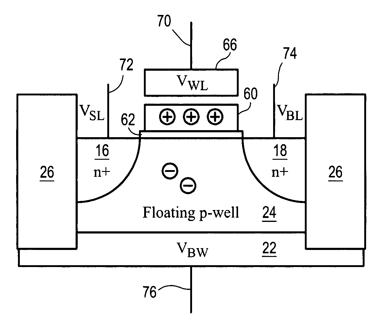
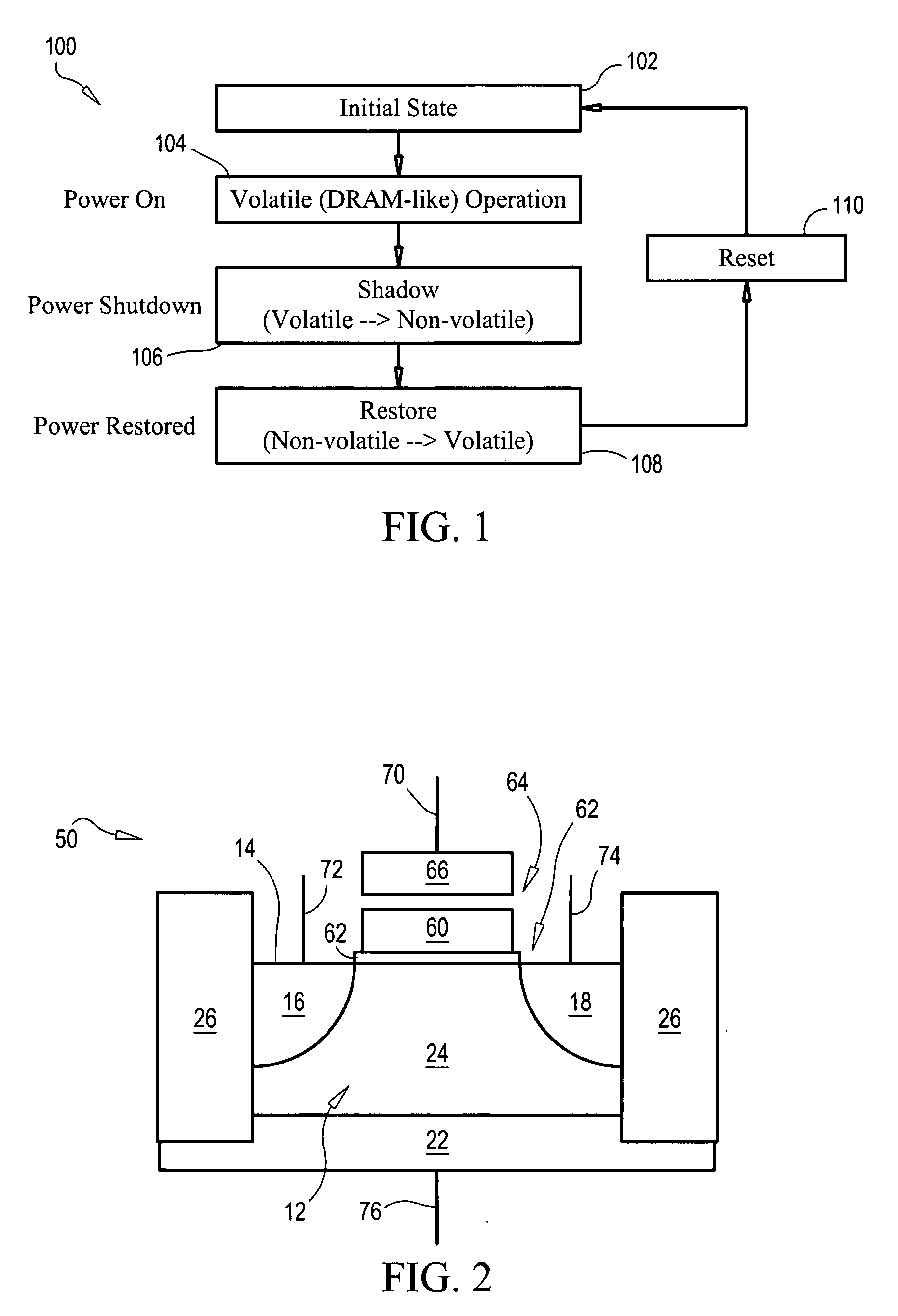
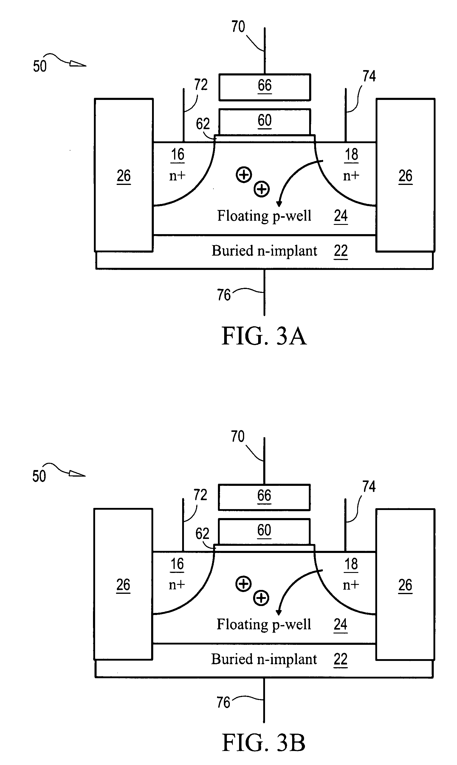
Semiconductor memory having both volatile and non-volatile modes and methods of operation. A semiconductor memory cell includes a substrate having a first conductivity type; a first region embedded in the substrate at a first location of the substrate and having a second conductivity type; a second region embedded in the substrate at a second location the substrate and have the second conductivity type, such that at least a portion of the substrate having the first conductivity type is located between the first and second locations and functions as a floating body to store data in volatile memory; a floating gate or trapping layer positioned in between the first and second locations and above a surface of the substrate and insulated from the surface by an insulating layer; the floating gate or trapping layer being configured to receive transfer of data stored by the volatile memory and store the data as nonvolatile memory in the floating gate or trapping layer upon interruption of power to the memory cell; and a control gate positioned above the floating gate or trapping layer and a second insulating layer between the floating gate or trapping layer and the control gate.

Description

CROSS-REFERENCE[0001]This application claims the benefit of U.S. Provisional Application No. 60 / 861,778, filed Nov. 29, 2006, which application is incorporated herein, in its entirety, by reference thereto.FIELD OF THE INVENTION[0002]The present inventions relates to semiconductor memory technology. More specifically, the present invention relates to semiconductor memory having both volatile and non-volatile semiconductor memory features.BACKGROUND OF THE INVENTION[0003]Semiconductor memory devices are used extensively to store data. Memory devices can be characterized according to two general types: volatile and non-volatile. Volatile memory devices such as static random access memory (SRAM) and dynamic random access memory (DRAM) lose data that is stored therein when power is not continuously supplied thereto.[0004]Non-volatile memory devices, such as flash erasable programmable read only memory (Flash EPROM) device, retain stored data even in the absence of power supplied thereto...

Claims


Application Information

Patent Timeline
IPC IPC(8): G11C16/04H01L29/788
CPCG11C11/404G11C14/0018G11C16/0416G11C2211/4016H01L29/78H01L29/66833H01L29/7841H01L29/7881G11C11/40H01L29/66825H10B12/20
Inventor WIDJAJA, YUNIARTO
Owner ZENO SEMICON
Why Eureka
Try Eureka