Circuits to delay a signal from ddr-sdram memory device including an automatic phase error correction
- Summary
- Abstract
- Description
- Claims
- Application Information
AI Technical Summary
Benefits of technology
Problems solved by technology
Method used
Image
Examples
Embodiment Construction
[0031]Persons of ordinary skill in the art will realize that the following description of the present invention is illustrative only and not in any way limiting. Other embodiments of the invention will readily suggest themselves to such skilled persons.
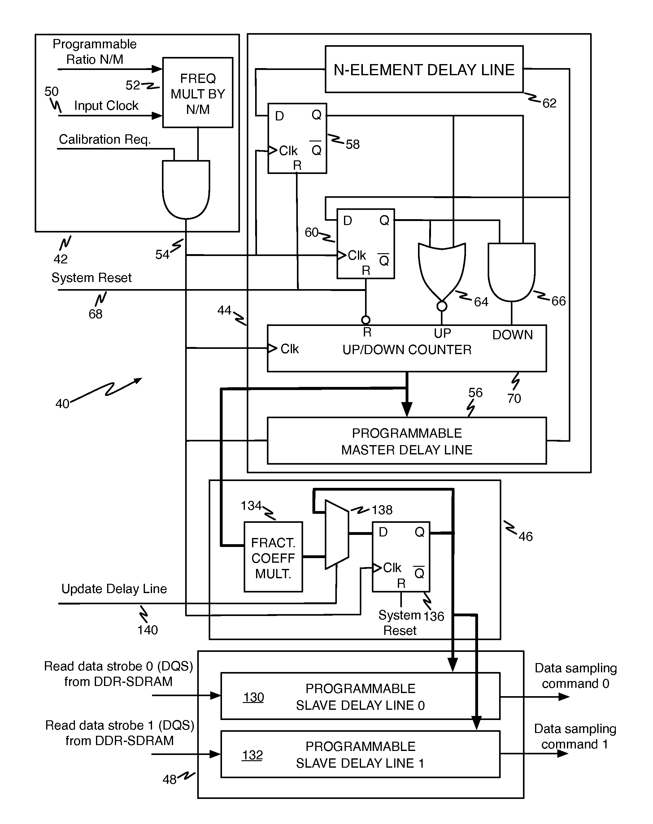
[0032]Referring now to FIG. 4, a block diagram illustrates a typical environment in which the present invention may be employed. FIG. 4 shows a system including a microcontroller 10 connected to a DDR-SDRAM device 12 through a DDR memory controller 14. An input clock signal, shown at reference numeral 16, provides a clock reference signal to DQS delay circuitry 18. The function of DQS delay circuitry 18 is to delay the DQS(0) and DQS(1) signals from DDR-SDRAM device 12 to produce a delayed DQS(0) and a delayed DQS(1) signal to control reading data from DDR-SDRAM device 12. It is to a DQS delay circuitry 18 that the present invention is directed.
[0033]As may be seen from an examination of FIG. 4, the delayed DQS(0) and delayed DQS(1) s...
PUM
 Abstract
Description
Claims
Application Information


