

Silicon Wafer And Method For Manufacturing The Same
a technology of silicon wafers and manufacturing methods, applied in the field of silicon wafers, can solve the problems of causing circuit breaks or other device problems, and significantly reducing the strength of silicon wafers, so as to achieve the effect of significantly suppressing the occurrence of slippage and warpage in the wafer manufacturing process
Active Publication Date: 2008-06-05
SILTRONIC AG
View PDF4 Cites 17 Cited by
- Summary
- Abstract
- Description
- Claims
- Application Information
AI Technical Summary
Benefits of technology
[0014]Therefore, a problem to be solved by the present invention is to provide a silicon wafer in which both slip dislocations and warpage are suppressed by the wafer manufacturing process, and a method for manufacturing such wafers. These and other objects have been achieved by examining wafers having BMDs with a wide distribut
Problems solved by technology
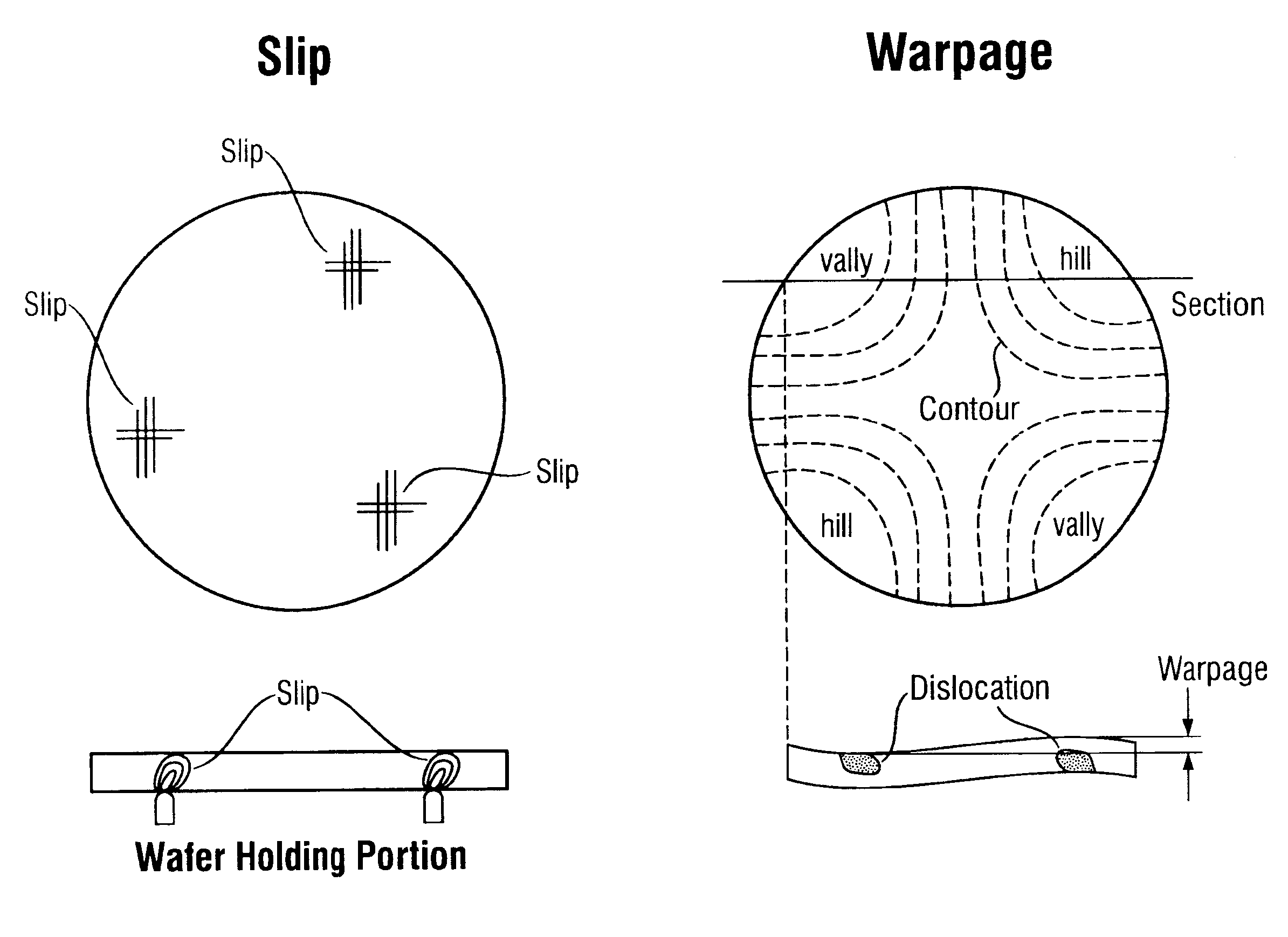
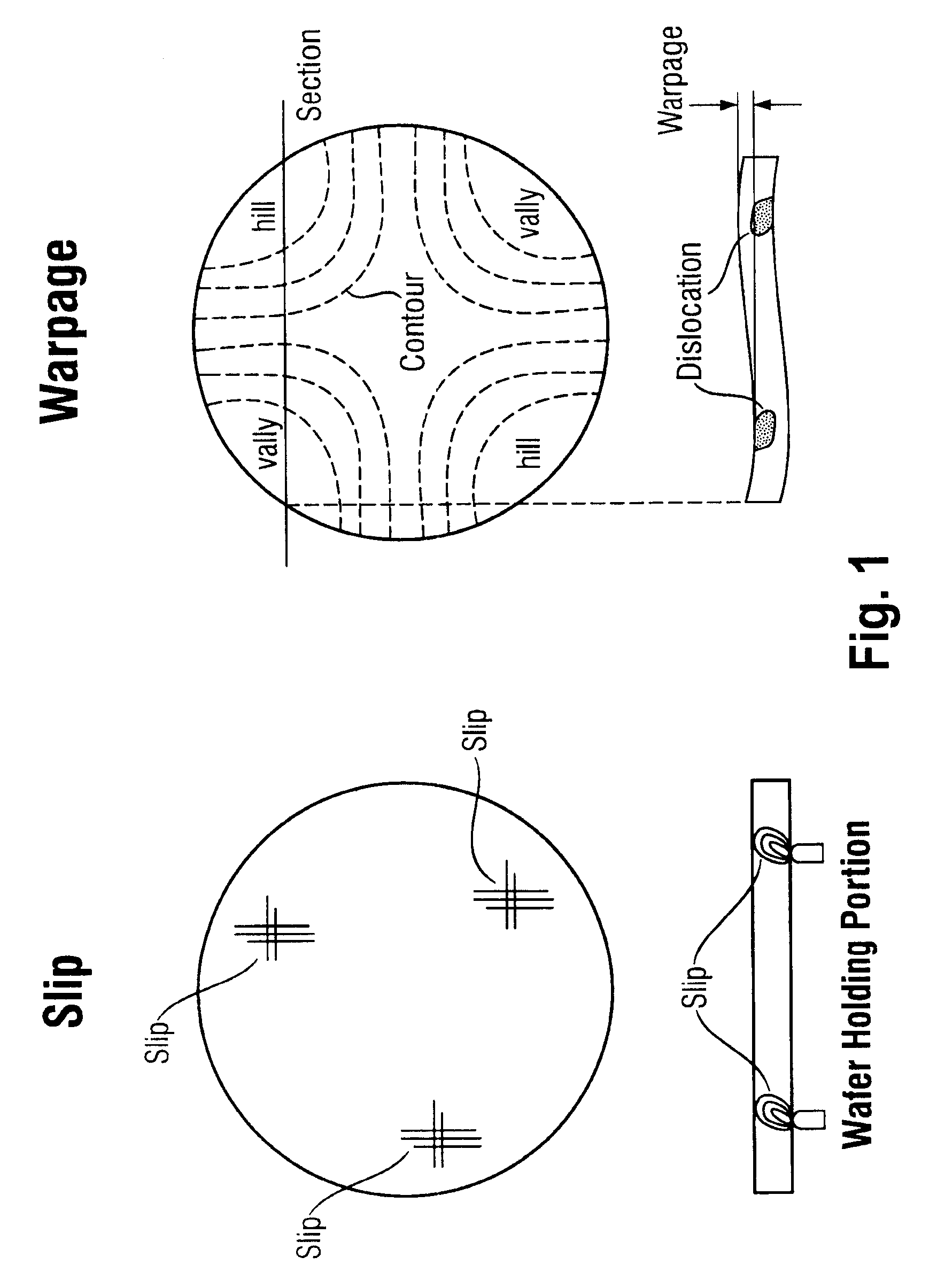
The reason for this requirements is that when crystal defects are present on a surface on which a circuit is formed, circuit breaks or other device problems are caused by the defects.
As a result, restraint of dislocation defect extension on the wafer front and back faces is significantly reduced, and dislocation defects (“slip defects”) easily propagate into the bulk from fine flaws on the front and back surfaces created in the anneal step, which results in lowering the strength of the silicon wafer due to propagation of slip dislocations.
When the strength of the silicon wafer is reduced, the wafers may be damaged or broken during subsequent manufacturing steps.
In the conventional method described in JP-A-10-98047, reduction in the strength of silicon wafers has not been addressed, and therefore
Method used
View moreImage
Smart ImageViewing Examples

Examples
 PUM
| Property | Measurement | Unit |
|---|---|---|
| Temperature | aaaaa | aaaaa |
| Temperature | aaaaa | aaaaa |
| Temperature | aaaaa | aaaaa |
Abstract
Silicon wafers and a process for their manufacture wherein both slip dislocation and occurrence of warpage are suppressed include heat treatment to provide wafers having plate-shaped BMDs, a density of BMDs whose diagonal lengths are in a range of 10 nm to 120 nm, of BMDs present in the bulk of the wafer at a distance of 50 μm or more is 1×10¹¹/cm3 or more, and the density of BMDs whose diagonal lengths are 750 nm or more in the wafer bulk is 1×10⁷/cm3 or less, and the interstitial oxygen concentration is 5×10¹⁷ atoms/cm3 or less. The process involves low and high temperature heat treating at under defined temperature ramping rates.
Description
BACKGROUND OF THE INVENTION[0001]1. Field of the Invention[0002]The present invention relates to a silicon wafer where both slip dislocation and warpage occurrence are suppressed, and to a method for manufacturing the same.[0003]2. Background Art[0004]Silicon wafers used as a substrate for a semiconductor devices or the like are manufactured by slicing a silicon single-crystal ingot into wafers and performing heat treatment, mirror finishing, and other processing steps to form a finished wafer. One method for manufacturing silicon single-crystal ingots is the Czochralski method (“CZ method”), for example. The CZ method is used for the majority of silicon single-crystal ingot manufacturing because of the ease of obtaining single-crystal ingots with large diameters, and because defects can be controlled relatively easily.[0005]A silicon single-crystal (“CZ-Si”) pulled by the CZ method includes crystal defects called “grown-in defects”. The CZ-Si contains interstitial oxygen in a super...
Claims
Login to View More Application Information
Patent Timeline
 IPC IPC(8): B32B7/02H01L21/22
CPCC30B29/06C30B33/00Y10T428/24942Y10T428/24992H01L21/3225H01L21/20
InventorNAKAI, KATSUHIKOFUKUSHIMA, SEI
OwnerSILTRONIC AG