Semiconductor device and manufacturing method of the same

a technology of semiconductor devices and manufacturing methods, applied in semiconductor devices, radiation controlled devices, electrical apparatus, etc., can solve the problems of limited current flow of space charges, inability to maintain off-operation, and limitation in reducing on-resistance, so as to suppress the occurrence of punch-through phenomena

Inactive Publication Date: 2010-12-30
NEC CORP
View PDF9 Cites 17 Cited by
  • Summary
  • Abstract
  • Description
  • Claims
  • Application Information

AI Technical Summary

Benefits of technology

[0056]According to the present invention, the occurrence of a punch-through phenomenon can be suppressed.

Problems solved by technology

However, when the depletion layer in the p-type GaN layer (103) reaches the whole region of the p-type GaN layer (103), a space charge limited current flows because of a punch-through phenomenon and the off-operation cannot be maintained.
Therefore, there is a limitation in reducing the on-resistance by thinning the p-type GaN layer (103).

Method used


Image

  • Semiconductor device and manufacturing method of the same
  • Semiconductor device and manufacturing method of the same
  • Semiconductor device and manufacturing method of the same

Examples


embodiment 1

Structure of a Semiconductor Device

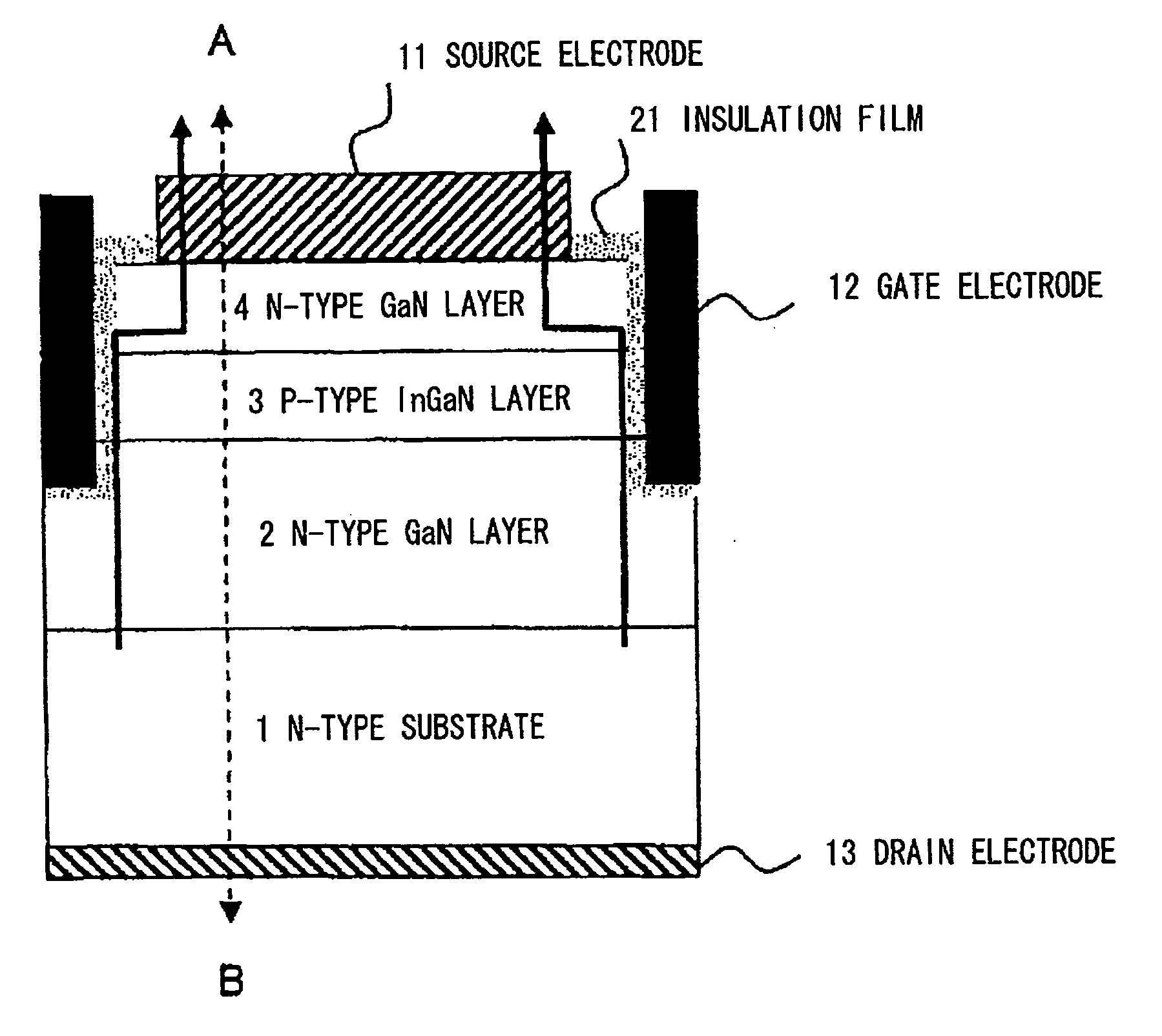
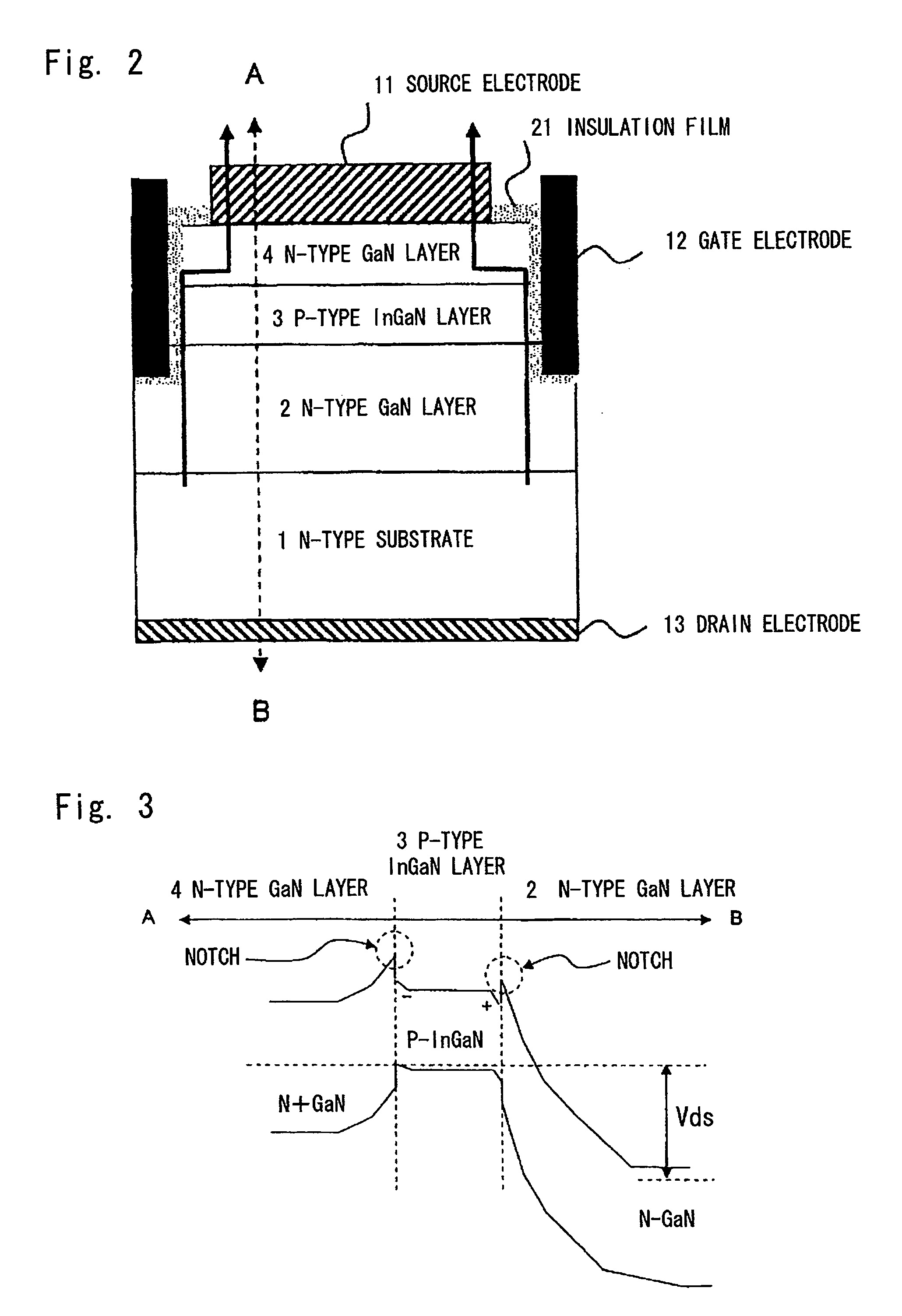
[0061]First, a structure of a semiconductor device according to the exemplary embodiment is explained with reference to FIG. 2. Note that FIG. 2 schematically illustrates a semiconductor structure in a vertical type GaN FET which serves as a semiconductor device according to the exemplary embodiment.

[0062]In the vertical type GaN FET according to the exemplary embodiment, an n-type GaN layer (2), a p-type InGaN layer (3), an n-type GaN layer (4) are sequentially formed on an n-type substrate (1) composed of such as Si. Further, a drain electrode (13) in ohmic contact is formed under the n-type substrate (1). Further, a source electrode (11) in ohmic contact is formed on the n-type GaN layer (4). Further, there is a gate electrode (12) in contact with the n-type GaN layer (4), the p-type InGaN layer (3), and the n-type GaN layer (2) through a gate insulation film (21). In the vertical type FET of the exemplary embodiment, the gate electrode (12) and...

embodiment 2

[0074]Next, the second exemplary embodiment is explained hereinafter.

[0075]In the first exemplary embodiment, the n-type GaN layer (2) and the p-type InGaN layer (3) is formed from different compositions, and a positive polarized charge (+) is generated on the under interface of the p-type InGaN layer (3) and a negative polarized charge (−) is generated on the upper interface thereof. Therefore, the polarized charge generated in the p-type InGaN layer (3) raises a band energy. This makes it possible to thin the p-type InGaN layer (3) with suppressing the occurrence of a punch-through phenomenon.

[0076]In the second exemplary embodiment, as shown in FIG. 4, the n-type InGaN (5) and the p-type InGaN layer (3) are formed from the same composition. It is thereby possible to prevent notches from being formed on the boundary surface between the n-type InGaN layer (5) and the p-type InGaN layer (3). Hereinafter, with reference to FIG. 4 and FIG. 5, the second exemplary embodiment is explain...

embodiment 3

[0087]Next, the third exemplary embodiment is explained hereinafter.

[0088]In the second exemplary embodiment, as shown in FIG. 4, the n-type InGaN layer (5) and the p-type InGaN layer (3) are formed from the same composition to prevent notches from being, formed on the boundary surface between the n-type InGaN layer (5) and the p-type InGaN layer (3).

[0089]In the third exemplary embodiment, as shown in FIG. 6, a composition modulation layer (6) where the composition is continuously or gradually changed is formed between the n-type GaN layer (2) and the p-type InGaN layer (3). This makes it possible to provide the suppression effect of a punch-through phenomenon by the polarized charge generated in the p-type InGaN layer (3) in a manner similar to the first exemplary embodiment. Further, it is possible to prevent notches from being formed between the n-type GaN layer (2) and the p-type InGaN layer (3). Hereinafter, with reference to FIG. 6 and FIG. 7, the third exemplary embodiment i...


PUM


Abstract

A semiconductor device capable of suppressing the occurrence of a punch-through phenomenon is provided. A first n-type conductive layer (2′) is formed on a substrate (1′). A p-type conductive layer (3′) is formed thereon. A second n-type conductive layer (4′) is formed thereon. On the under surface of the substrate (1′), there is a drain electrode (13′) connected to the first n-type conductive layer (2′). On the upper surface of the substrate (1′), there is a source electrode (11′) in ohmic contact with the second n-type conductive layer (4′), and a gate electrode (12′) in contact with the first n-type conductive layer (2′), p-type conductive layer (3′), the second n-type conductive layer (4′) through an insulation film (21′). The gate electrode (12′) and the source electrode (11′) are alternately arranged. The p-type conductive layer (3′) includes In.

Description

TECHNICAL FIELD[0001]The present invention relates to a semiconductor device and a manufacturing method of the same.BACKGROUND ART[0002]First, a semiconductor device related to the present invention is explained hereinafter with reference to FIG. 8. FIG. 8 schematically illustrates a semiconductor structure of a vertical type GaN field effect transistor (hereinafter called vertical type GaN FET). Note that a vertical type GaN FET shown in FIG. 8 is disclosed in Non patent literature 1, for example.[0003]In the vertical type GaN FET shown in FIG. 8, an n-type GaN layer (102) is formed on a high concentration n-type GaN layer (101). A p-type GaN layer (103) is formed thereon. An n-type GaN layer (104) is formed thereon. A source electrode (111) in ohmic contact is formed thereon. Further, a drain electrode (113) in ohmic contact is formed on the high concentration n-type GaN layer (101) which is exposed by removing a semiconductor layer. Furthermore, a gate electrode (112) is formed o...

Claims


Application Information

Patent Timeline
Patent Type & Authority Applications(United States)
IPC IPC(8): H01L29/205H01L29/78H01L21/336
CPCH01L29/2003H01L29/201H01L29/7813H01L29/66734H01L29/205
Inventor OKAMOTO, YASUHIROOTA, KAZUKIINOUE, TAKASHIMIYAMOTO, HIRONOBUNAKAYAMA, TATSUOANDO, YUJI
Owner NEC CORP
Why Eureka
Try Eureka